Semiconductor package structure and method for manufacturing the same

a technology of semiconductors and packaging, applied in the direction of individual semiconductor device testing, semiconductor/solid-state device testing/measurement, instruments, etc., can solve the problems of increased system level complexity within the package, difficulty in achieving high yield, and increased electrical, thermal and mechanical complexity

Active Publication Date: 2010-01-14
ZAWASHIRO DIGITAL INNOVATIONS
View PDF6 Cites 113 Cited by
  • Summary
  • Abstract
  • Description
  • Claims
  • Application Information

AI Technical Summary

Problems solved by technology

Stacking different types of chips is also possible but at the cost of greater electrical, thermal and mechanical complexity as well as the difficulties to achieve high yields with increased system level complexity within the package.
Additionally, the use of TSP structures decreases the need for complicated wire bonding of stacked chip because each chip need not be electrically connected to the substrate [unit] independently as is currently the case for memory devices in mass production of stacked packages.
Typically, high performance and small form factor packages are costly to manufacture.
Additionally, there is no general approach to the TSP bonding method.
New process and materials increase the complexity and yield loss in the implementation of stacked chip using TSP with resulting increases in cost.
Irrespective of the process and integration choices that are made, there is considerable risk and uncertainty in implementation.
As a result of increased complexity and possible yield loss, stacked packages using TSPs will be more expensive to fabricate.

Method used


Image

  • Semiconductor package structure and method for manufacturing the same
  • Semiconductor package structure and method for manufacturing the same
  • Semiconductor package structure and method for manufacturing the same

Examples


first embodiment

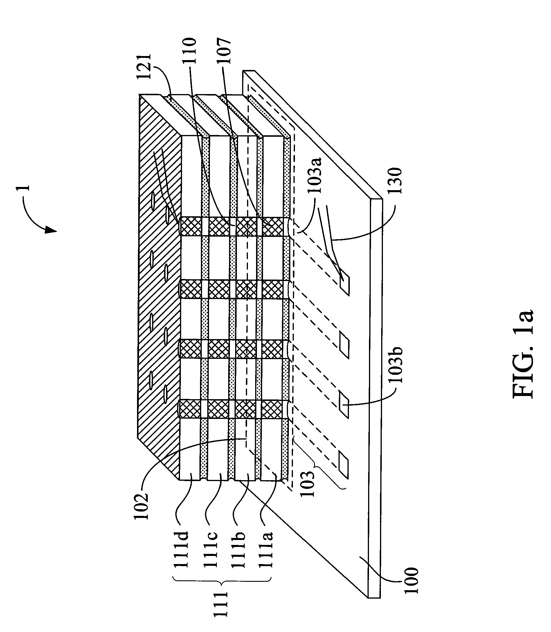
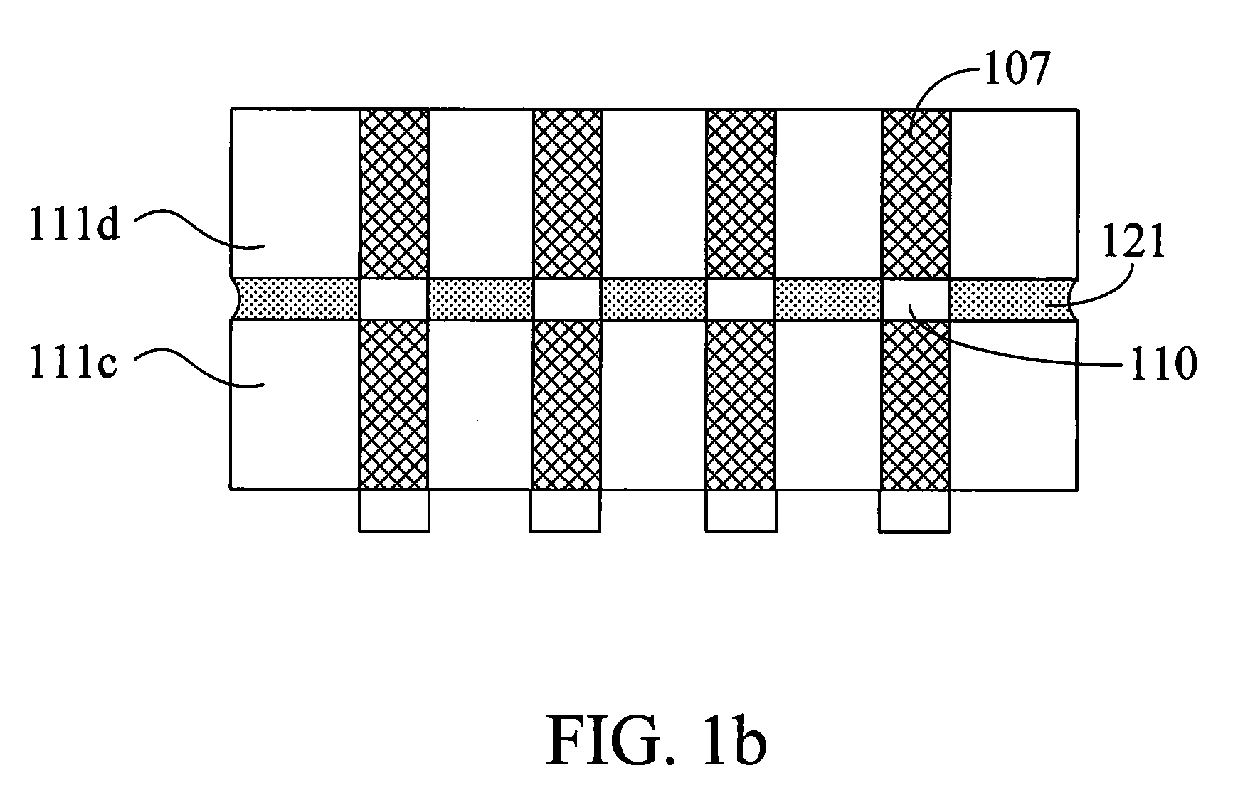
[0031]FIG. 1a is a partial cross sectional view of a semiconductor package structure 1 according to this invention. The semiconductor package structure 1 comprises a substrate unit 100, a first chip stack structure 111, and sealing layers 121. The substrate unit 100 has a chip mounting area 102 defined thereupon and a circuit structure 103 formed thereon. The circuit structure 103 has a plurality of connecting circuits 103a, a plurality of test pads 103b, and a plurality of bonding pads (not shown). Each of the bonding pads (not shown) is arranged within the chip mounting area 102, and each of the test pads 103b is arranged outside of the chip mounting area 102. The connecting circuits 103a operatively connect the bonding pads (not shown) and the test pads 103b. In this embodiment, an isolating protection layer (not shown) formed on the substrate unit 100 exposes only the bonding pads and the test pads 103b for external contacts but covers the connecting circuits 103a to eliminate c...

second embodiment

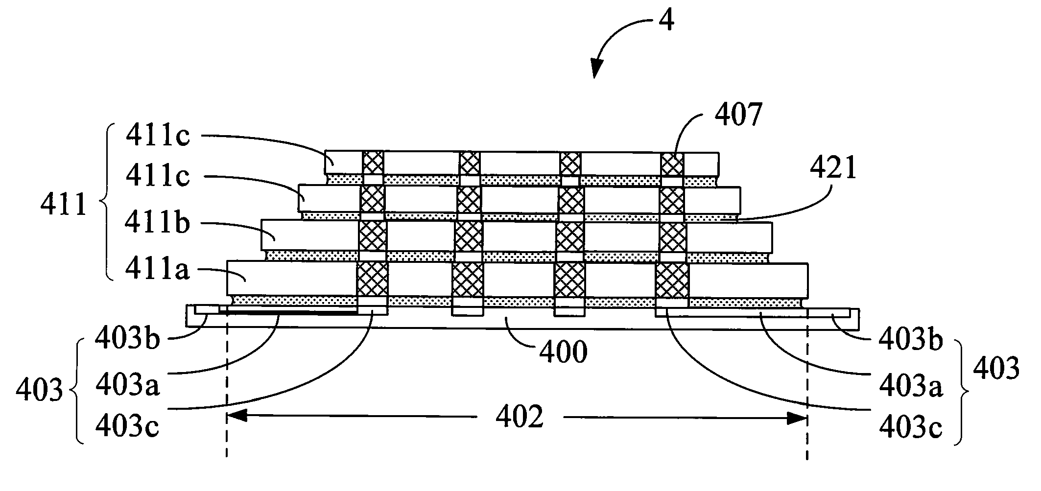
[0044]FIG. 3 is a partial cross sectional view of a semiconductor package structure 3 according to this invention. The semiconductor package structure 3 comprises a substrate unit 300, a first chip stack structure 311, and sealing layers 321. The substrate unit 300 comprises a chip mounting area 302 defined thereupon and a circuit structure 303 formed thereon. The first chip stack structure 311 is mounted on the chip mounting area 302 of the substrate unit 300. The first chip stack structure 311 comprises a plurality of chips 311a, 311b, and 311c, and each of the chips 311a, 311b, and 311c has an upper surface, a bottom surface opposite the upper surface, and a plurality of through silicon plugs 307 disposed therein to form electrical interconnections between the upper surface and the bottom surface.

[0045]The most prominent difference from the first embodiment is that the second chip 311b and the third chip 311c are both mounted on and electrically connected to the adjacent first ch...

fifth embodiment

[0049]FIG. 6 is a partial cross sectional view of a semiconductor package structure 6 according to this invention. The semiconductor package structure 6 comprises a substrate unit 600, a first chip stack structure 611, a second chip stack structure 613, an insulating adhesive layer 615, sealing layers 621, and bonding wires 640. The substrate unit 600 has a chip mounting area 602 defined thereupon and a circuit structure 603 formed thereon. The circuit structure 603 has a plurality of connecting circuits 603a, a plurality of test pads 603b, and a plurality of first bonding pads (not shown), and a plurality of second bonding pads 603c. Each of the first bonding pads (not shown) is arranged within the chip mounting area 602, and each of the test pads 603b is arranged outside of the chip mounting area 602. The connecting circuits 603a connect the first bonding pads (not shown) and the test pads 603b, and the connecting circuits 603a are covered with an isolating protection layer (not s...


PUM


Abstract

Semiconductor package structures and methods for manufacturing the same are provided. The semiconductor package structure comprises a substrate unit and a first chip stack structure. The substrate unit comprises a circuit structure having test pads. The first chip stack structure comprises chips, and each of the chips has a plurality of through silicon plugs. The through silicon plugs of two adjacent chips are electrically connected and further electrically connected to the test pads of the substrate unit for electrical testing. Another semiconductor package structure provided by the present invention comprises a first semiconductor chip and a second semiconductor chip. Each of the semiconductor chips has test pads for electrical testing and a plurality of through silicon plugs connecting to the test pads. The second semiconductor chip is mounted on the first semiconductor chip, and a portion of the through silicon plugs of two semiconductor chips are electrically connected with each other.

Description

[0001]This application claims priorities to Taiwan Patent Application No. 098100319 filed on Jan. 6, 2009, and U.S. Provisional Application No. 61 / 079,900 filed on Jul. 11, 2008, the disclosures of which are incorporated herein by reference in their entiretyCROSS-REFERENCES TO RELATED APPLICATIONS[0002]Not applicable.BACKGROUND OF THE INVENTION[0003]1. Field of the Invention[0004]The present invention provides a semiconductor package structure, a method for manufacturing the same. In particular, the present invention provides a semiconductor package structure comprising chips which are vertically stacked and electrically interconnected by through silicon plugs to a substrate unit using ultrasonic bonding methods. Additionally, test pads can be provided on the substrate unit or the chip to facilitate in process control. Also a method is disclosed that utilizes existing infrastructure thereby reducing cost.[0005]2. Descriptions of the Related Art[0006]The trend in advanced semiconduct...

Claims


Application Information

Patent Timeline
Patent Type & Authority Applications(United States)
IPC IPC(8): H01L23/52H01L23/538H01L21/98H01L21/768
CPCH01L23/481H01L25/0657H01L2924/07802H01L2924/30107H01L2924/01087H01L24/48H01L2924/09701H01L25/50H01L2224/48091H01L2225/06513H01L2225/06517H01L2225/06562H01L2225/06596H01L2924/01046H01L2924/01079H01L2924/00014H01L2924/00H01L2224/05554H01L2224/16145H01L2224/32145H01L2224/73204H01L2924/14H01L2224/45099H01L2224/45015H01L2924/207
Inventor WANG, DAVID WEILIU, AN-HONGTSAI, HAO-YINHUANG, HSIANG-MINGLEE, YI-CHANGHO, SHU-CHING
Owner ZAWASHIRO DIGITAL INNOVATIONS
Why Eureka
Try Eureka