Resistive memory device and method for manufacturing the same

a technology of resistive memory and memory device, which is applied in the direction of semiconductor devices, bulk negative resistance effect devices, electrical equipment, etc., can solve the problems of insufficient oxygen around the upper electrode interface, and the inability to return from a set state. achieve the effect of improving the endurance of the resistive memory devi

Active Publication Date: 2010-01-28
SK HYNIX INC
View PDF4 Cites 31 Cited by
  • Summary
  • Abstract
  • Description
  • Claims
  • Application Information

AI Technical Summary

Benefits of technology

[0009]Embodiments of the present invention are directed to providing a resistive memory device which can prohibit the out diffusion of oxygen in the interface of the upper electrode to prevent set-stuck phenomenon occurring upon the operation of the resistive memory device and thereby improving the endurance of the resistive memory device, and a method for manufacturing the same.

Problems solved by technology

However, repeated write / erase operations of the resistive memory device may cause a set-stuck phenomenon, in which it is impossible to returns from a set state to a reset state.
However, since the oxygen of the upper electrode interface is diffused out as time passes, the oxygen around the upper electrode interface becomes insufficient.
As a result, the resistive memory device is weak with respect to an endurance of framework, and this property makes it difficult to substantially utilize the resistive memory device as a memory device.

Method used


Image

  • Resistive memory device and method for manufacturing the same
  • Resistive memory device and method for manufacturing the same

Examples


first embodiment

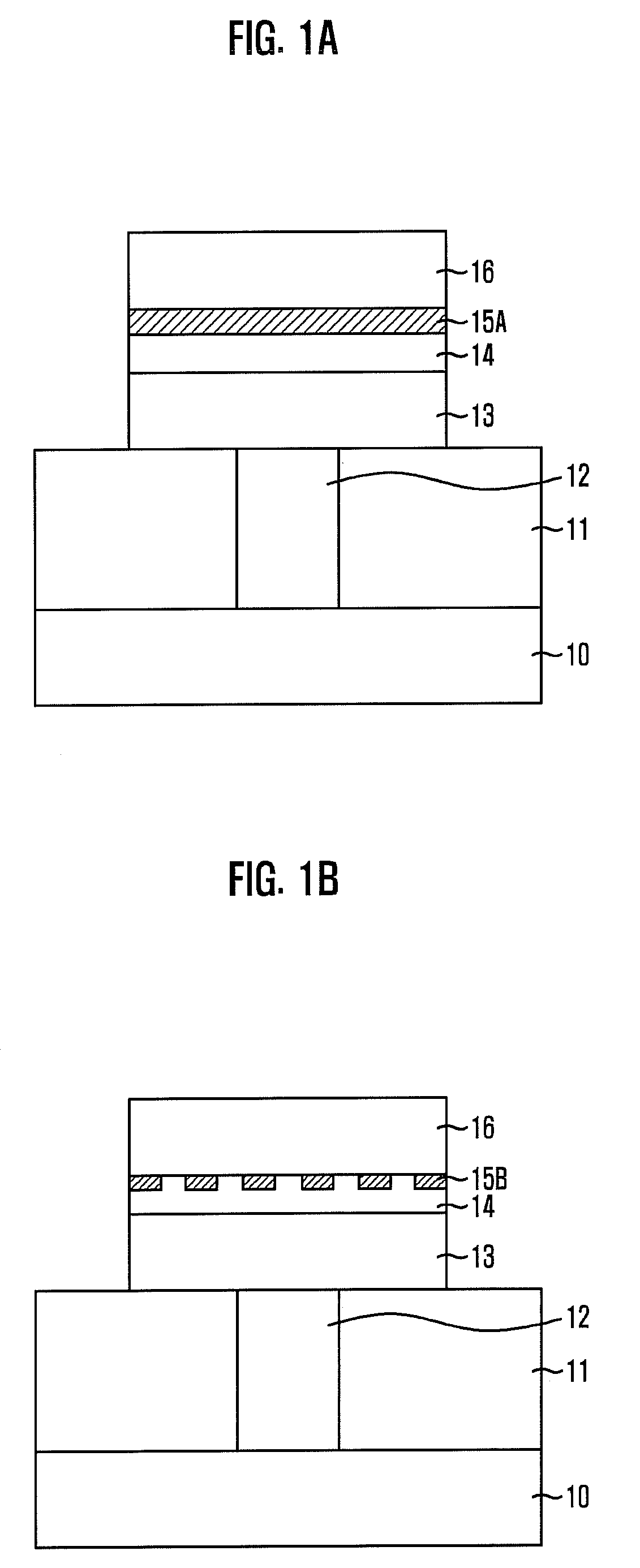
[0020]The method of manufacturing the resistive memory device according to the present invention is described hereinafter with reference to FIG. 1A.

[0021]As shown in FIG. 1A, an insulating film 11 is formed over a substrate 10 with a predetermined lower structure, and a contact plug 12 which is connected to the substrate 10 through the insulating film 11 is formed.

[0022]Then, the lower electrode 13 which covers the contact plug 12 is formed over the insulating film 11, and the resistive layer 14 is then formed over the lower electrode 13.

[0023]Subsequently, a thin film-type oxygen-diffusion barrier pattern 15A is formed by depositing a metal film over the resistive layer 14. In this case, the deposition thickness of the metal thin film may range from approximately 10 Å to approximately 200 Å.

[0024]Subsequently, an upper electrode 16 is formed over the thin film-type oxygen-diffusion barrier pattern 15A.

second embodiment

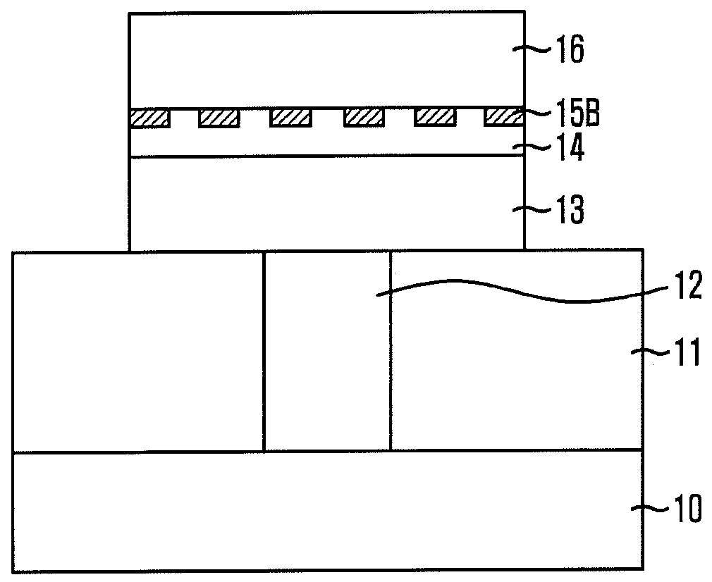
[0025]A method of manufacturing a resistive memory device according to the present invention is described hereinafter with reference to FIG. 1B.

[0026]As shown in FIG. 1B, an insulating film 11 is formed over a substrate 10 with a predetermined lower structure, and then the contact plug 12 which is connected to the substrate 10 through the insulating film 11 is formed.

[0027]Then, a lower electrode 13 which covers the contact plug 12 is formed over the insulating film 11, and a resistive layer 14 is formed over the lower electrode 13.

[0028]Then, a metal thin film is deposited on the resistive layer 14, with respect to which a thermal processing is then performed. As a result of the performance of the thermal processing, the metal thin film coagulates in a form of dot. As a result, a dot-type oxygen-diffusion barrier pattern 15B is formed over the resistive layer 14. In this case, the deposition thickness of the metal thin film may range from approximately 10 Å to approximately 200 Å, ...


PUM


Abstract

A resistive memory device and a method for manufacturing the same are disclosed. The resistive memory device includes a lower electrode formed over a substrate, a resistive layer disposed over the lower electrode, an upper electrode formed over the resistive layer, and an oxygen-diffusion barrier pattern provided in an interface between the resistive layer and the upper electrode. The above-described resistive memory device and a method for manufacturing the same may prevent the out diffusion of oxygen in the interface of the upper electrode to avoid set-stuck phenomenon occurring upon the operation of the resistive memory device, thereby improving the endurance of the resistive memory device.

Description

CROSS-REFERENCE TO RELATED APPLICATIONS[0001]The present invention claims priority of Korean patent application number 10-2008-0072475, filed on Jul. 24, 2008, respectively, which is incorporated by reference in its entirety.BACKGROUND OF THE INVENTION[0002]The present invention relates to a technology of manufacturing a semiconductor device, and more particularly, to a resistive memory device which utilizes a change in resistance, such as in nonvolatile Resistive Random Access Memory (ReRAM) devices, and a method for manufacturing the same.[0003]Recently, researchers are actively studying next-generation semiconductor memory devices which can replace Dynamic Random Access Memory (DRAM) and flash memory.[0004]One of such next-generation semiconductor memory devices is a resistive memory device utilizing a material whose resistance changes rapidly according to an applied bias to switch between at least two different resistance states, that is, a resistive layer. As a resistive layer ...

Claims


Application Information

Patent Timeline
Patent Type & Authority Applications(United States)
IPC IPC(8): H01L29/68H01L21/44
CPCH01L45/08H01L45/1233H01L45/147H01L45/145H01L45/146H01L45/1253H10N70/24H10N70/826H10N70/841H10N70/8833H10N70/883H10N70/8836H01L27/105
Inventor LEE, YU-JIN
Owner SK HYNIX INC
Why Eureka
Try Eureka