
Electrically programmable device with embedded eeprom and method for making thereof

Active Publication Date: 2010-01-28
SEMICON MFG INT (SHANGHAI) CORP
View PDF2 Cites 278 Cited by
  • Summary
  • Abstract
  • Description
  • Claims
  • Application Information

AI Technical Summary

Benefits of technology

[0010]In a specific embodiment, the invention provides a method for making a semiconductor device. The method includes providing a substrate including a first device region and a second device region, growing a first gate oxide layer in the first device region and the second device region, and forming a first diffusion region in the first device region and a second diffusion region and a third diffusion region in the second device region. Additionally, the method includes implanting a first plurality of ions to form a fourth diffusion region in the first device region and a fifth diffusion region in the second device region. The fourth diffusion region overlaps with the first diffusion region. Moreover, the method includes forming a first gate in the first device region and a second gate and a third gate in the second device region, and depositing a first dielectric layer on the first gate, the second gate, the third gate, and the first gate oxide layer. Also, the method includes etching a first part and a second part of the first dielectric layer and a first part of the first gate oxide layer in the first device region. The first part of the first dielectric layer is on the first gate, and the second part of the first dielectric layer is on the first part of the first gate oxide layer. Additionally, the method includes growing an inter-gate oxide layer and a second gate oxide layer in the first device region. The inter-gate oxide layer is on the first gate, and the second gate oxide layer is on the substrate. Moreover, the method includes forming a fourth gate on at least the second oxide layer, the inter-gate oxide layer, and the first dielectric layer in the first device region, forming a fifth gate on the first dielectric layer in the second device region, and implanting a second plurality of ions to form a plurality of source regions and a plurality of drain regions. The etching a first part and a second part of the first dielectric layer and a first part of the first gate oxide layer in the first device region is free from removing any part of the first dielectric layer in the second device region.

Problems solved by technology

An IC fabrication facility can cost hundreds of millions, or even billions, of dollars.
Moreover, the output of the fabrication facility also depends on the complexity of the fabrication process.
For example, additional masking steps and / or additional ion implantation steps may significantly reduce the throughput and increase the cost.
Although fabless chip companies and foundry services have increased through the years, many limitations still exist.
For example, it is difficult to efficiently make erasable programmable read-only memory (EPROM) with embedded EEPROM.

Method used


Image

  • Electrically programmable device with embedded eeprom and method for making thereof
  • Electrically programmable device with embedded eeprom and method for making thereof
  • Electrically programmable device with embedded eeprom and method for making thereof

Examples


Embodiment Construction

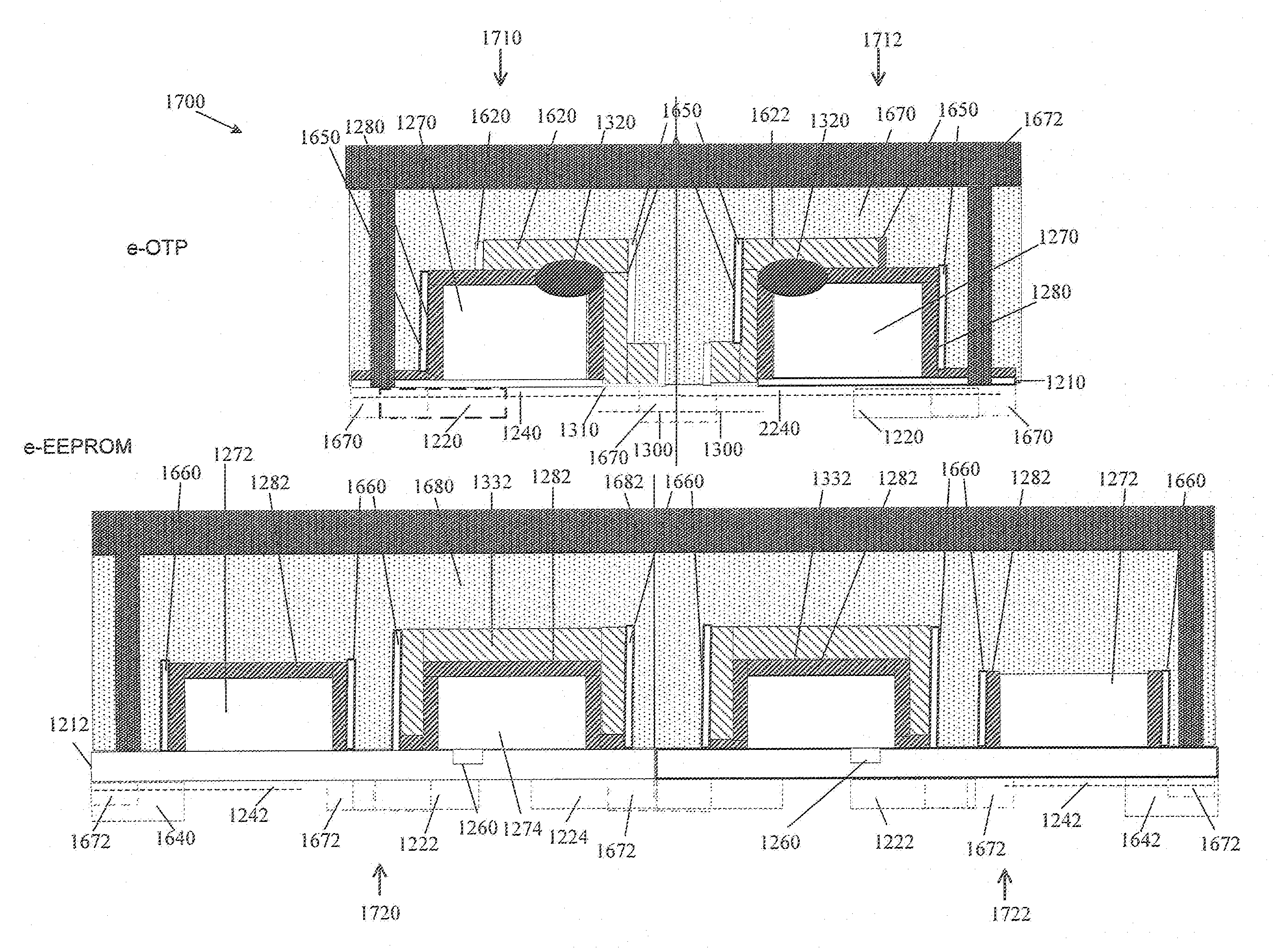
[0033]The present invention is directed to integrated circuits and their processing for the manufacture of semiconductor devices. More particularly, the invention provides a programmable device with embedded electrically-erasable programmable read-only memory (EEPROM) and method for making thereof. Merely by way of example, the invention has been applied to one-time programmable (OTP) device with embedded EEPROM. But it would be recognized that the invention has a much broader range of applicability.

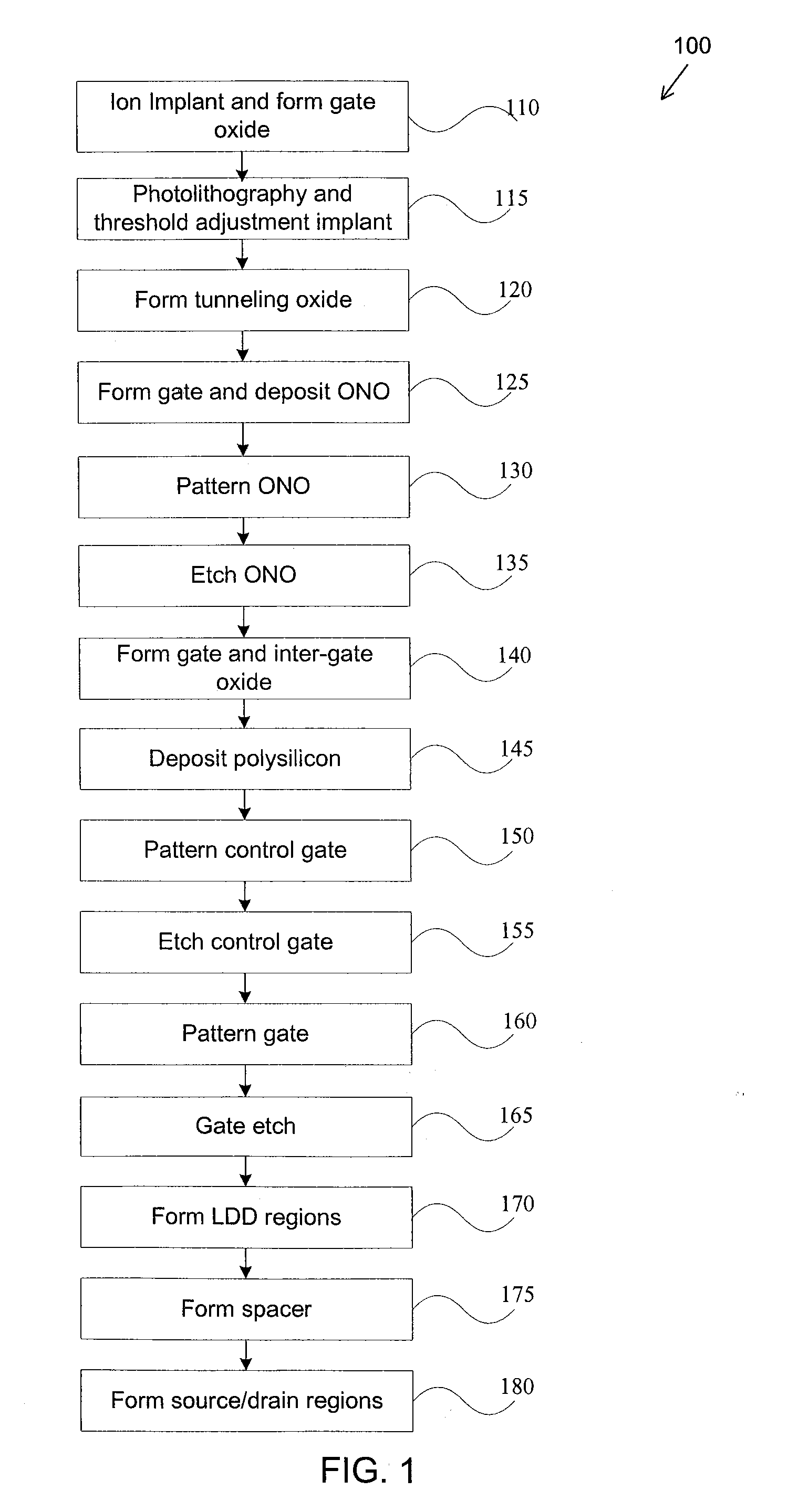
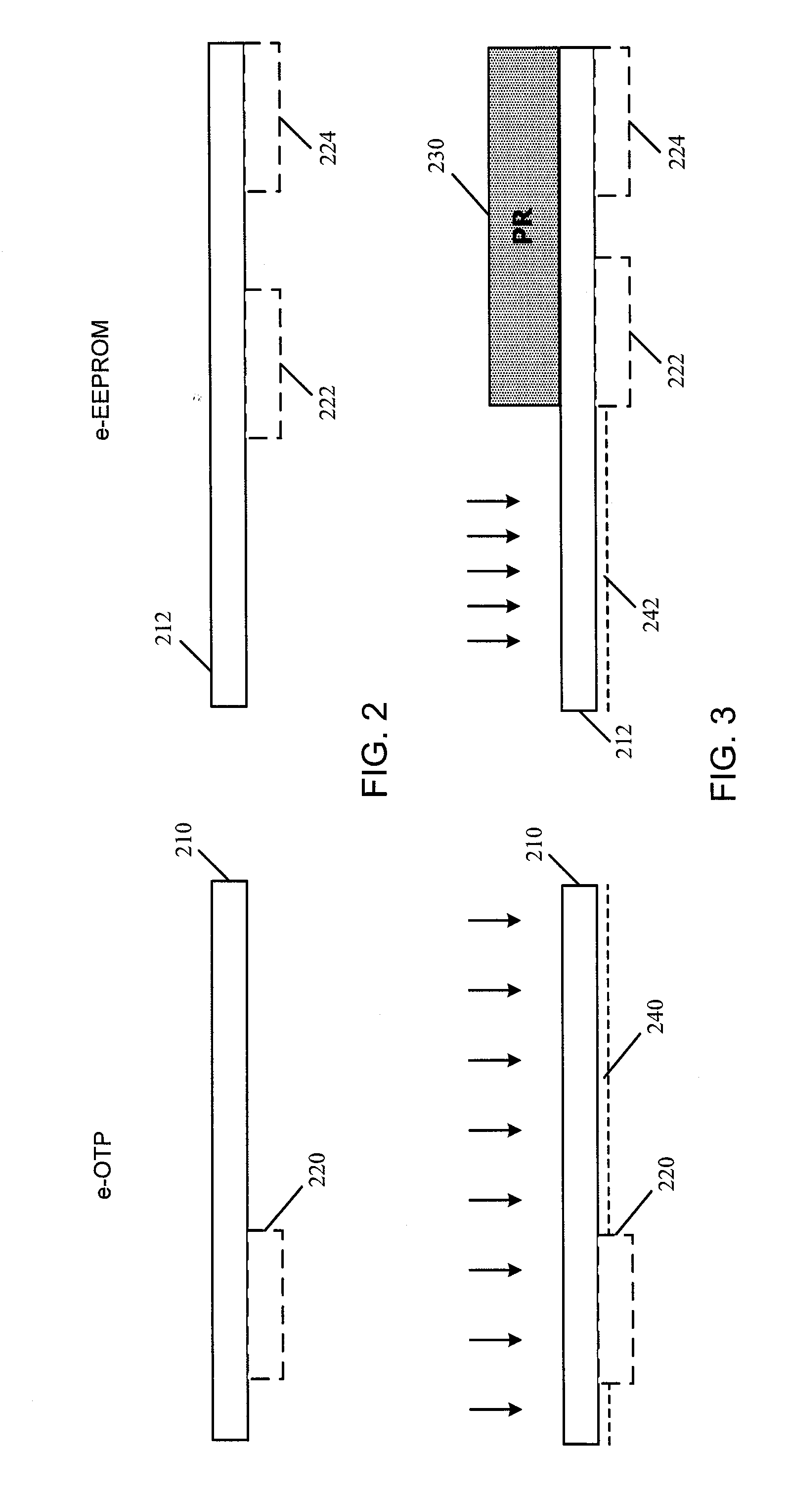
[0034]FIG. 1 is a simplified method for forming a programmable device according to an embodiment of the present invention. The method 100 includes at least the following processes:[0035]1. Process 110 for ion implantation and gate oxide formation;[0036]2. Process 115 for photolithography and ion implantation for threshold adjustment;[0037]3. Process 120 for forming tunneling oxide;[0038]4. Process 125 for gate and oxide-nitride-oxide formation;[0039]5. Process 130 for oxide-nitride-oxide...


PUM


Abstract

An electrically programmable device with embedded EEPROM and method for making thereof. The method includes providing a substrate including a first device region and a second device region, growing a first gate oxide layer in the first device region and the second device region, and forming a first diffusion region in the first device region and a second diffusion region and a third diffusion region in the second device region. Additionally, the method includes implanting a first plurality of ions to form a fourth diffusion region in the first device region and a fifth diffusion region in the second device region. The fourth diffusion region overlaps with the first diffusion region.

Description

CROSS-REFERENCES TO RELATED APPLICATIONS[0001]NOT APPLICABLESTATEMENT AS TO RIGHTS TO INVENTIONS MADE UNDER FEDERALLY SPONSORED RESEARCH OR DEVELOPMENT[0002]NOT APPLICABLEREFERENCE TO A “SEQUENCE LISTING,” A TABLE, OR A COMPUTER PROGRAM LISTING APPENDIX SUBMITTED ON A COMPACT DISK.[0003]NOT APPLICABLEBACKGROUND OF THE INVENTION[0004]The present invention is directed to integrated circuits and their processing for the manufacture of semiconductor devices. More particularly, the invention provides a programmable device with embedded electrically-erasable programmable read-only memory (EEPROM) and method for making thereof. Merely by way of example, the invention has been applied to one-time programmable (OTP) device with embedded EEPROM. But it would be recognized that the invention has a much broader range of applicability.[0005]Integrated circuits or “ICs” have evolved from a handful of interconnected devices fabricated on a single chip of silicon to millions of devices. Current ICs...

Claims


Application Information

Patent Timeline
IPC IPC(8): H01L27/115H01L21/8247
CPCH01L21/28273H01L27/11206H01L27/115H01L29/7883H01L27/11521H01L27/11524H01L29/42324H01L27/11519H01L29/40114H10B20/20H10B69/00H10B41/10H10B41/30H10B41/35
Inventor CHAN, YI-PENGHUANG, SHENG-HEYANG, ZHEN
Owner SEMICON MFG INT (SHANGHAI) CORP
Features
  • Generate Ideas
  • Intellectual Property
  • Life Sciences
  • Materials
  • Tech Scout
  • Unparalleled Data Quality
  • Higher Quality Content
  • 60% Fewer Hallucinations
Learn More