
Deposition methods for releasing stress buildup

a technology of stress buildup and deposition method, which is applied in the direction of semiconductor/solid-state device manufacturing, basic electric elements, electric apparatus, etc., can solve the problems of increasing the aspect ratio, progressively more difficult to fill gaps without leaving voids, and affecting the operation of the completed device, so as to reduce the bending effect of lines

Inactive Publication Date: 2010-01-28
APPLIED MATERIALS INC
View PDF12 Cites 8 Cited by
  • Summary
  • Abstract
  • Description
  • Claims
  • Application Information

AI Technical Summary

Benefits of technology

[0007]Embodiments of the invention pertain to methods for releasing a stress of a liner layer formed over a feature of a semiconductor structure. The stress release of the liner layer can desirably reduce the bending effect of lines of the feature that may result in sticking of the lines. By reducing the bending effect of the lines, a gapfill material can be desirably filled within gaps of the feature.
[0008]One embodiment of the invention provides a deposition method for releasing a stress buildup of a feature over a semiconductor substrate with dielectric material. The feature includes lines separated by a gap. The method includes forming a liner layer over the feature on the semiconductor substrate in a chamber. A stress of the liner layer over the feature is released to substantially reduce bending of the lines of the feature. A dielectric film is deposited over the stress-released liner layer to substantially fill the gap of the feature.

Problems solved by technology

One of the persistent challenges faced in the development of semiconductor technology is the desire to increase the density of circuit elements and interconnections on substrates without introducing spurious interactions between them.
As circuit densities increase, however, the widths of these gaps decrease, increase their aspect ratios and making it progressively more difficult to fill the gaps without leaving voids.
The formation of voids when the gap is not filled completely is undesirable because they may adversely affect operation of the completed device, such as by trapping impurities within the insulation material.
The high reactivity of the species in the plasma reduces the energy required for a chemical reaction to take place, and thus lowers the temperature required for such CVD processes when compared with conventional thermal CVD processes.
Such dep / etch / dep processes have also been used with PECVD techniques, but some thermal and PECVD techniques are still unable to fill gaps having very large aspect ratios even by cycling deposition and etching steps.
Originally, the application of dep / etch / dep processes to HDP-CVD was considered counterintuitive because, unlike PECVD processes, the high density of ionic species in the plasma during HDP-CVD processes already causes there to be sputtering of a film while it is being deposited.
If the gaps of STI structures are sealed, the dep / etch / dep processes cannot provide a gapfill material within the gaps for isolation.

Method used


Image

  • Deposition methods for releasing stress buildup
  • Deposition methods for releasing stress buildup
  • Deposition methods for releasing stress buildup

Examples


Embodiment Construction

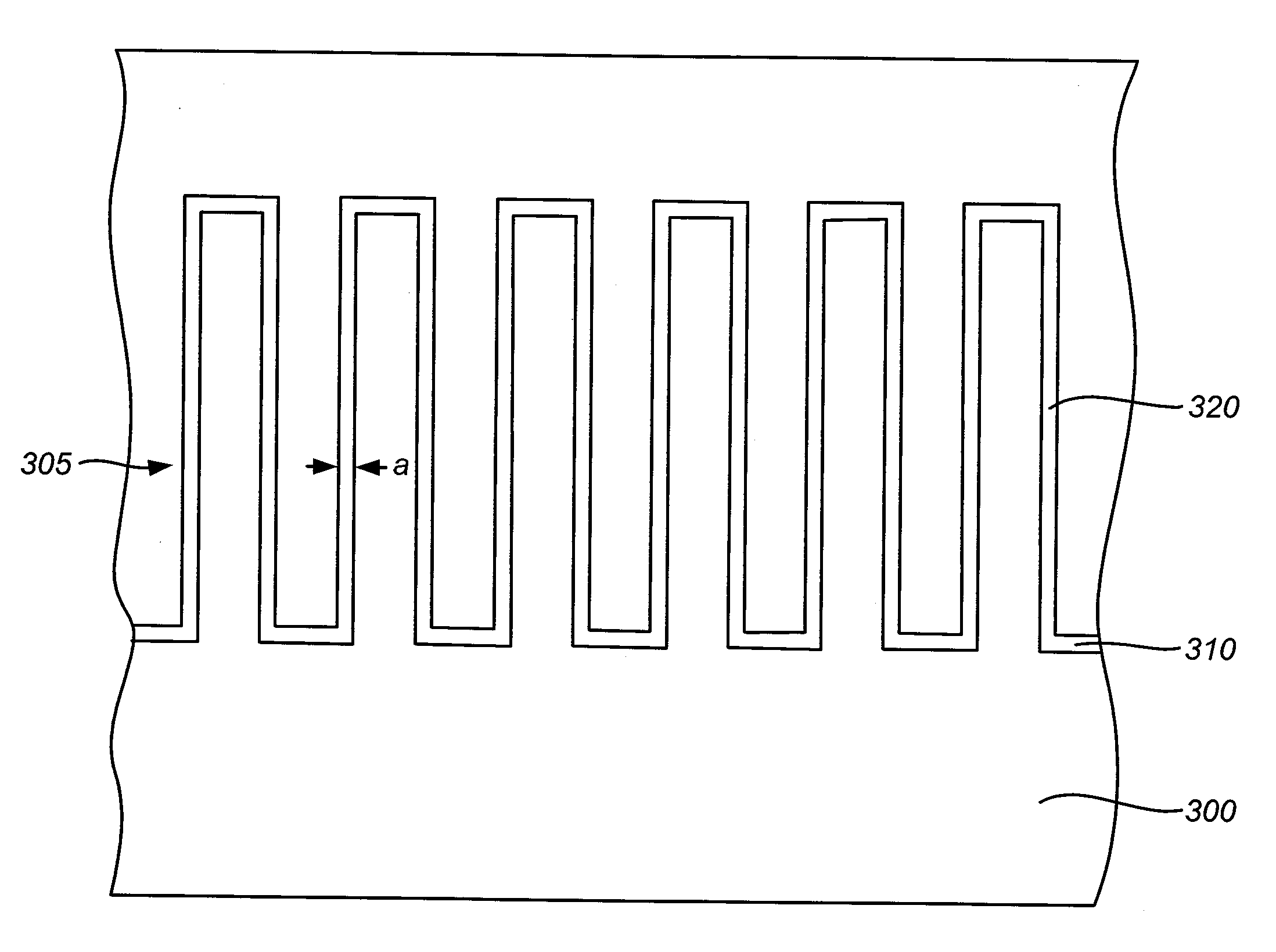
[0015]The invention relates to methods for semiconductor manufacturing. More particularly, the invention relates to gapfill methods for reducing bending effect of semiconductor structures. The method may include forming a liner layer over a feature over a semiconductor structure. Prior to filling a gapfill material in gaps of the feature, the method releases a stress of the liner layer formed over the feature. The feature can include lines with a width of about 40 nm or less and / or have an aspect ratio of about 10 or more. The stress release of the liner layer can desirably reduce the bending effect of lines of the feature that may stick the lines of the feature. By reducing the bending effect of the lines, the gapfill material can be desirably filled within gaps of the feature.

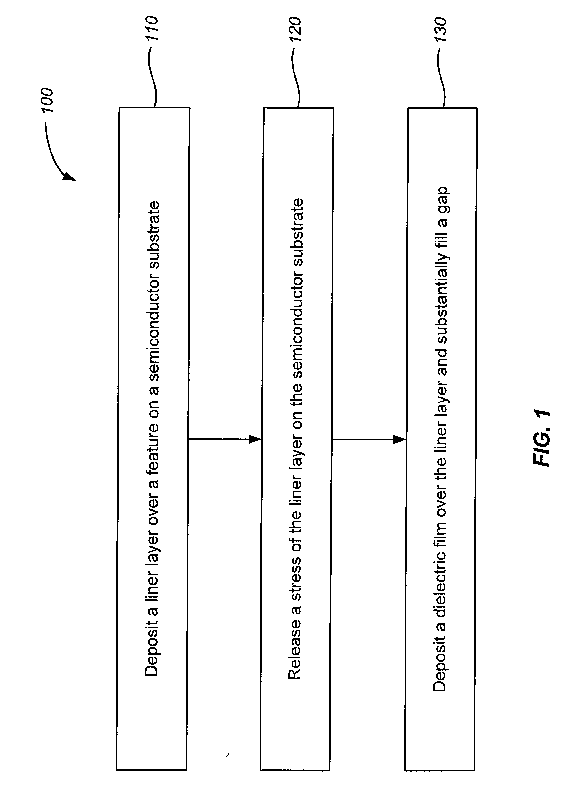
[0016]FIG. 1 is a flowchart illustrating a deposition method according to an embodiment of the invention. In FIG. 1, method 100 includes step 110 for depositing a liner layer over a feature on a semiconductor...


PUM


Abstract

A deposition method for releasing a stress buildup of a feature over a semiconductor substrate with dielectric material is provided. The feature includes lines separated by a gap. The method includes forming a liner layer over the feature on the semiconductor substrate in a chamber. A stress of the liner layer over the feature is released to substantially reduce bending of the lines of the feature. A dielectric film is deposited over the stress-released liner layer to substantially fill the gap of the feature.

Description

FIELD OF THE INVENTION[0001]The invention relates to methods for semiconductor manufacturing. More particularly, the invention relates to gapfill methods for reducing bending effect of semiconductor structures.BACKGROUND OF THE INVENTION[0002]One of the persistent challenges faced in the development of semiconductor technology is the desire to increase the density of circuit elements and interconnections on substrates without introducing spurious interactions between them. Unwanted interactions are typically prevented by providing gaps or trenches that are filled with electrically insulation material to isolate the elements both physically and electrically. As circuit densities increase, however, the widths of these gaps decrease, increase their aspect ratios and making it progressively more difficult to fill the gaps without leaving voids. The formation of voids when the gap is not filled completely is undesirable because they may adversely affect operation of the completed device,...

Claims


Application Information

Patent Timeline
Patent Type & Authority Applications(United States)
IPC IPC(8): H01L21/762
CPCH01L21/76224H01L21/31
Inventor TANG, JINGINGLE, NITIN K.YUAN, ZHENGMININNI, ROSSELLA
Owner APPLIED MATERIALS INC
Learn More