Film formation apparatus and film formation method using the same

a film formation apparatus and film technology, applied in the direction of packaging, paper/cardboard containers, transportation and packaging, etc., can solve the problems of insufficient adhesion between the glass substrate and the mask, the mask and the glass substrate may not be easily separated from each other, and the quality of the mask is affected, so as to reduce the misalignment in the plane direction and good dimensional accuracy

Inactive Publication Date: 2010-02-04
CANON KK +1
View PDF4 Cites 11 Cited by
  • Summary
  • Abstract
  • Description
  • Claims
  • Application Information

AI Technical Summary

Benefits of technology

[0007]In view of the problem described above, the present invention has an object of providing a film formation apparatus capable of forming a pixel pattern with good dimensional accuracy and with reduced misalignment in a plane direction between a substrate and a mask when the substrate is pressed against the mask, and a film formation method using the film formation apparatus.
[0009]According to the film formation apparatus and the film formation method using the film formation apparatus according to the present invention, in the step of pressing the substrate against the mask to improve adhesiveness between the mask and the substrate, misalignment in a plane direction between the substrate and the mask may be suppressed. As a result, a pixel pattern arranged on the substrate may be formed with reduced misalignment in a plane direction and with good dimensional accuracy.

Problems solved by technology

Therefore, even slight misalignment in a plane direction between a pixel pattern formed on the glass substrate and a mask or insufficient adhesion between the glass substrate and the mask for vapor deposition disadvantageously degrades quality.
In particular, it is known that the insufficient adhesion between the glass substrate and the mask is also caused by slight distortion of the mask or the sag of the mask itself under its own weight.
As a result, in some cases, the mask and the glass substrate may not be easily separated away from each other.
On the other hand, when a magnetic force is small, there is fear that a gap may be generated between the mask and the substrate to cause a vapor-deposited film to flow into the gap.
In the method described in Japanese Patent Application Laid-Open No. 2005-158571, however, it is difficult to control to press the substrate in a direction vertical to the substrate in a strict manner when the substrate is dynamically pressed against the mask.
Even with a slight shift of a pressing direction from the vertical direction, there is a fear that a force in the plane direction may be applied to the substrate to cause the misalignment in the plane direction between the substrate and the mask.
As a result, the misalignment in the plane direction between the pixel pattern formed on the substrate and the pattern of the mask adversely occurs.

Method used


Image

  • Film formation apparatus and film formation method using the same
  • Film formation apparatus and film formation method using the same
  • Film formation apparatus and film formation method using the same

Examples


example 1

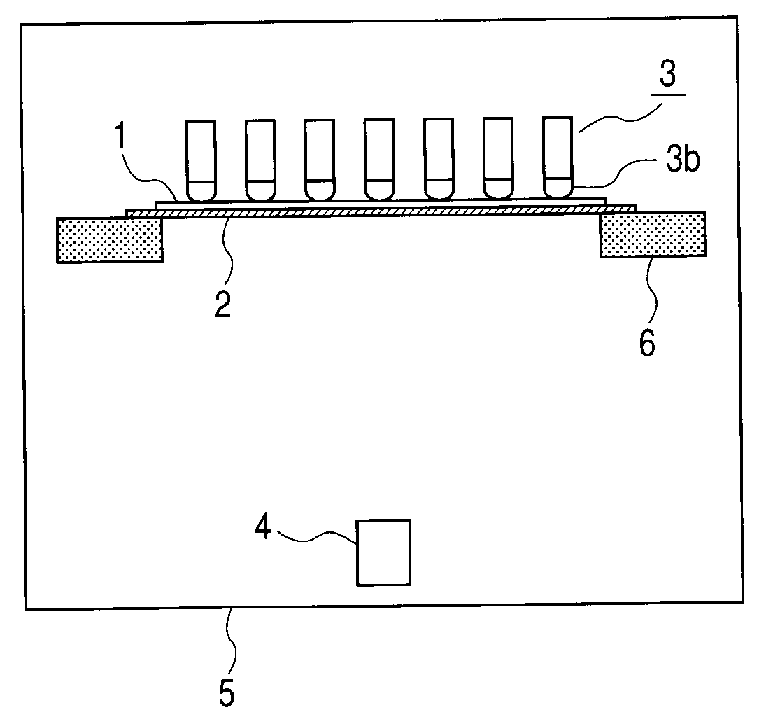
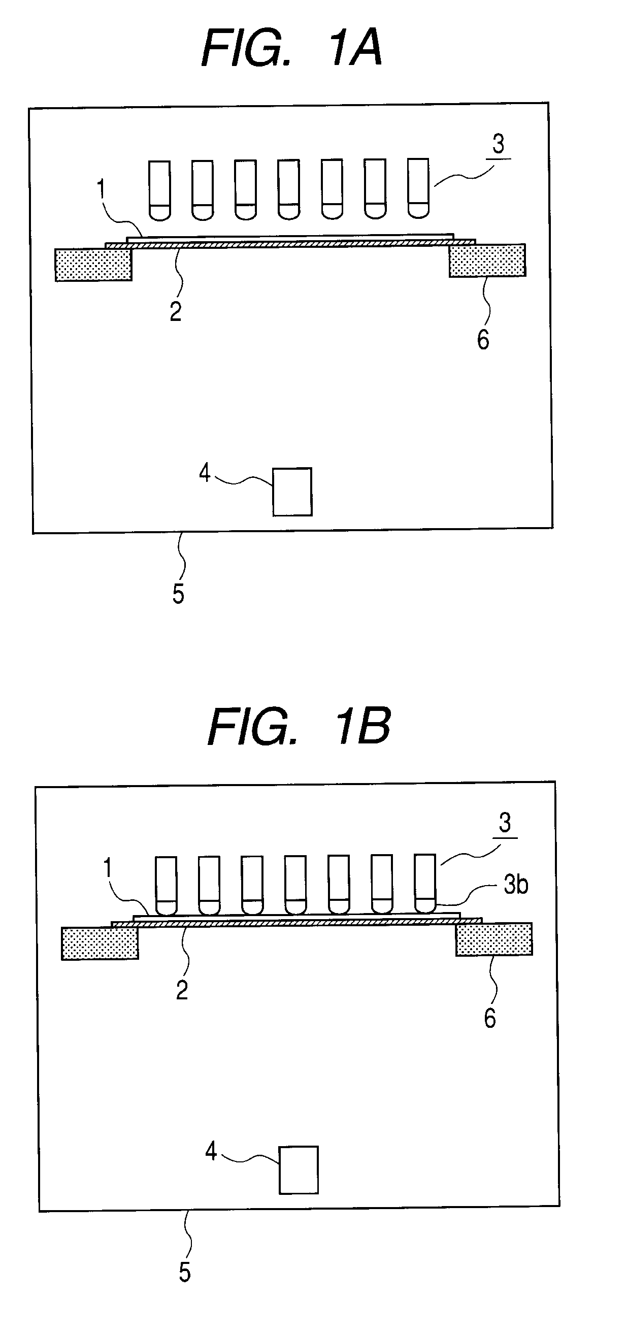
[0033]An organic EL device was fabricated on the glass substrate by the film formation apparatus. A known light-emitting material was placed in a film forming source which is the vapor depositing source. In the film forming chamber, the substrate was located with the surface, on which the film was to be formed, being oriented downward.

[0034]The glass substrate made of non-alkali glass with a thickness of 0.5 mm and dimensions of 400 mm×500 mm was used as the substrate. On the substrate, thin-film transistors (TFTs) and electrode wirings were formed in a matrix pattern by a conventional method. The size of one pixel was 30 μm×120 μm. A display region of the organic EL device was arranged in the center of the substrate to have dimensions of 350 mm×450 mm. For the mask, a tension was applied to the mask portion having a thickness of 50 μm and dimensions of 400 mm×500 mm to weld the mask portion to the frame having a thickness of 100 mm. The mask obtained by thus integrating the mask po...

example 2

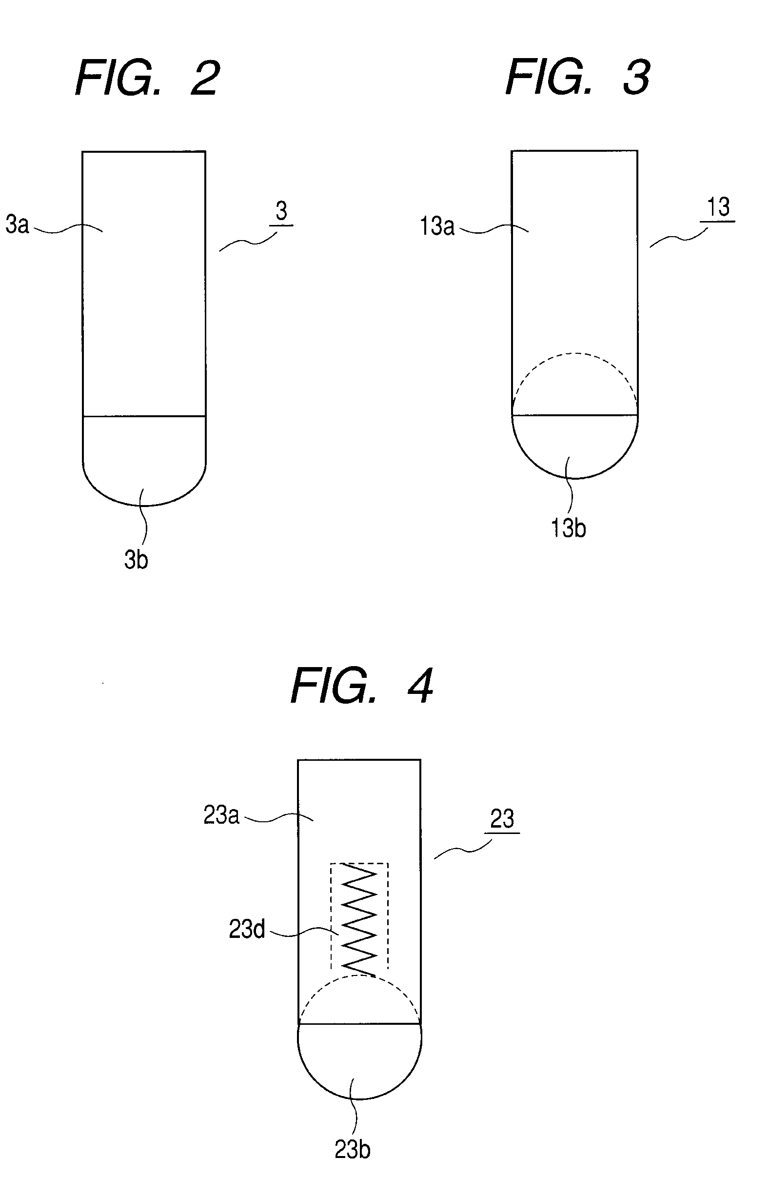
[0038]For the pressing body, a bar having a diameter of 10 mm was obtained by cutting SUS303. At a tip of the bar, which was to be brought into contact with the substrate, the rotating body made of SUS303 was attached as the contact member. The twenty-five pressing bodies were arranged to evenly press the twenty-five positions on the surface of the substrate. The height position of each of the pressing bodies was adjusted to allow the twenty-five pressing bodies to press the substrate almost simultaneously. The other conditions for the used mask and substrate were the same as those of Example 1.

[0039]As in the case of Example 1, anode electrodes were formed on the glass substrate including the TFTs, and by using the film formation apparatus and a known mask for vapor deposition, alignment between the substrate and the mask was performed in a vacuum state. After the alignment mechanism was operated to bring the substrate into contact with the mask, the pressing mechanism was lowered ...

example 3

[0041]For the pressing body, the bar having a diameter of 10 mm was obtained by cutting SUS303. At the tip of the bar, which was to be brought into contact with the substrate, the rotating body made of SUS303 was attached as the contact member. A spring which is the elastic body made of the fluorine resin was provided inside the main body of the pressing body to allow the force of the pressing body to be transmitted to the rotating body through the spring. The twenty-five pressing bodies were arranged to evenly press the twenty-five positions on the surface of the substrate. The height position of each of the pressing bodies was adjusted to allow the twenty-five pressing bodies to press the substrate almost simultaneously. The other conditions for the used mask and substrate were the same as those of Example 1.

[0042]As in the case of Example 1, the anode electrodes were formed on the glass substrate including the TFTs, and by using the film formation apparatus and a known mask for v...


PUM

PropertyMeasurementUnit
friction coefficientaaaaaaaaaa
thicknessaaaaaaaaaa
thicknessaaaaaaaaaa

Abstract

Provided are a film formation apparatus and a film formation method which are capable of forming a pixel pattern with good dimensional accuracy and with reduced misalignment in a plane direction between a substrate and a mask when the substrate is pressed against the mask. The film formation apparatus includes an alignment mechanism for aligning a substrate and a mask with each other and a pressing mechanism for pressing the substrate against the mask with a contact member provided to one end of a pressing body, which are provided in a vacuum chamber. After alignment between the substrate and the mask by the alignment mechanism, the contact member of the pressing body is brought into contact with a surface of the substrate, which is on a side opposite to the mask, to press the substrate.

Description

BACKGROUND OF THE INVENTION[0001]1. Field of the Invention[0002]The present invention relates to a film formation apparatus and a film formation method using the same.[0003]2. Description of the Related Art[0004]Conventionally, in a method of manufacturing an organic electroluminescence (EL) device, a mask film formation method of arranging a mask for film formation to be in close contact with a glass substrate is frequently used. As an example of such a mask film formation method, there is a mask vapor deposition method. According to the vapor deposition method, a pattern of an organic EL layer may be formed with good accuracy. In recent years, along with an increase in resolution of an organic EL panel, patterning becomes finer and finer. Therefore, even slight misalignment in a plane direction between a pixel pattern formed on the glass substrate and a mask or insufficient adhesion between the glass substrate and the mask for vapor deposition disadvantageously degrades quality.[0...

Claims


Application Information

Patent Timeline
Patent Type & Authority Applications(United States)
IPC IPC(8): C23C16/04B32B37/00
CPCC03C17/001C03C2218/15Y10T156/10C23C14/12C23C14/042
Inventor SODA, TAKEHIKOEIDA, MASATAKAMIYATA, KAZUSHI
Owner CANON KK
Why Eureka
Try Eureka