Electronic component built-in wiring board and method for radiating heat generated at the same

Active Publication Date: 2010-02-04
DAI NIPPON PRINTING CO LTD
View PDF14 Cites 37 Cited by
  • Summary
  • Abstract
  • Description
  • Claims
  • Application Information

AI Technical Summary

Benefits of technology

[0021]In a still another aspect of the present invention, the electronic component built-in wiring board has a metallic heat radiation plate formed at the same surface level as at least one of the plurality of wiring patterns and thermally contacted with the metallic body. In this case, since the heat emitted from the electronic component is radiated from the metallic heat radiation plate via the metallic body, the heat radiation effect can be enhanced.
[0022]In a further aspect of the present invention, the metallic body is a plurality of metallic bodies so that the plurality of metallic bodies are at least partially an

Problems solved by technology

In the electronic component built-in wiring board, however, the amount of heat of each of the electronic components, particularly, semiconductor components, which are embedded in the corresponding insulating layer, becomes large relatively.
On the other hand, since each of the insulating layers is made of low thermal conductivity material such as resin, the heat generated at the electronic component cannot be radiated outside effectively.
Therefore, the interior temperature of the wiring board is increased, thereby causing the destruction of the component mounting portion of the electronic component and damaging the con

Method used


Image

  • Electronic component built-in wiring board and method for radiating heat generated at the same
  • Electronic component built-in wiring board and method for radiating heat generated at the same
  • Electronic component built-in wiring board and method for radiating heat generated at the same

Examples


first embodiment

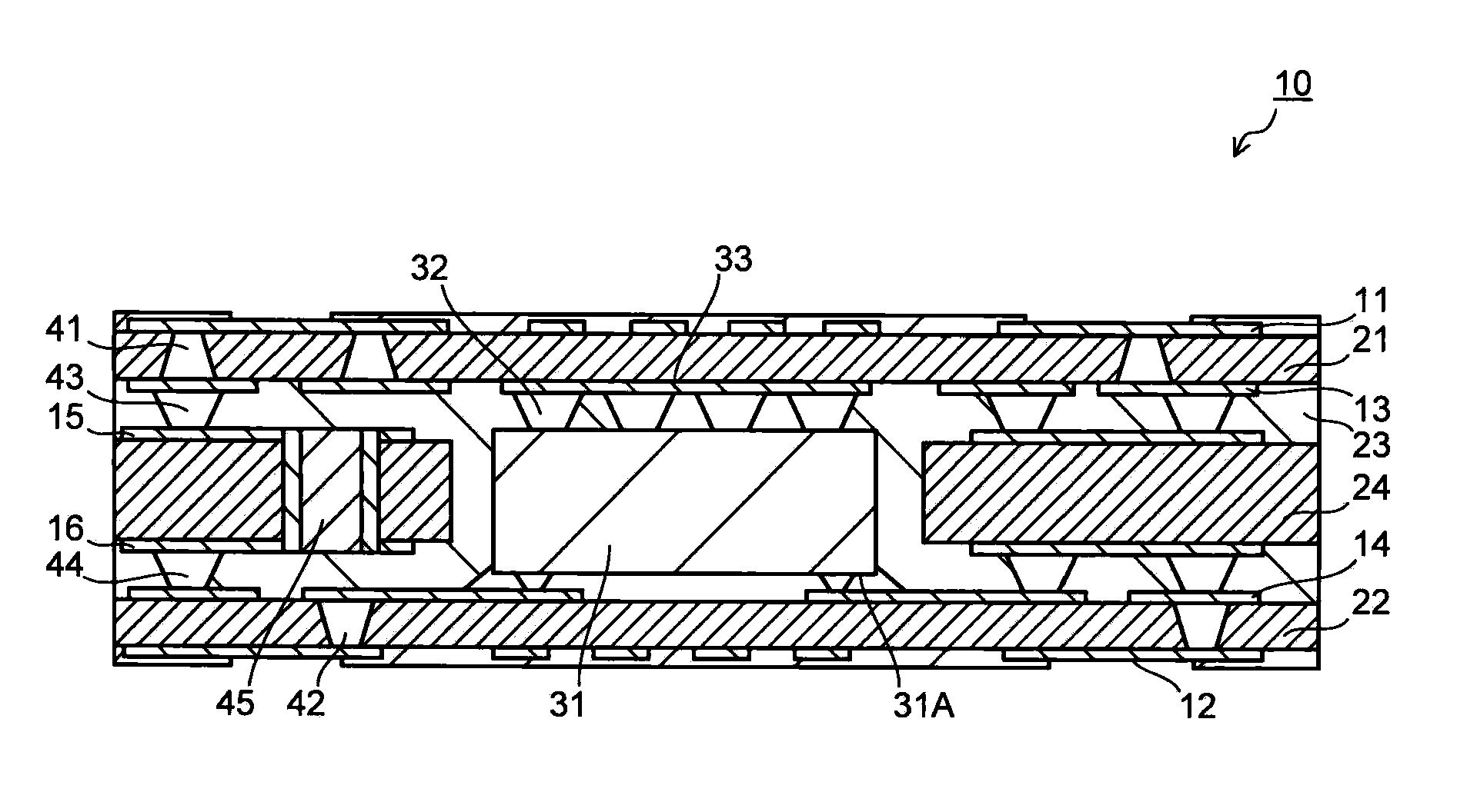
[0037]FIG. 1 is a cross sectional view showing the structure of an electronic component built-in wiring board according to a first embodiment. The electronic component built-in wiring board 10 shown in FIG. 1 includes a first wiring pattern 11 and a second wiring pattern 12 which are positioned at the main surface and the rear surface of the wiring board 10 and almost parallel to one another, and a third wiring pattern 13 and a fourth wiring pattern 14 which are disposed at the inside of the first wiring pattern 11 and the second wiring pattern 12 and almost parallel to one another and to the first wiring pattern 11, the second wiring pattern 12.

[0038]A first insulating layer 21 is disposed between the first wiring pattern 11 and the third wiring pattern 13, and a second insulating layer 22 is disposed between the second wiring pattern 12 and the fourth wiring pattern 14. A third insulating layer 23 is disposed between the third wiring pattern 13 and the fourth wiring pattern 14. An...

second embodiment

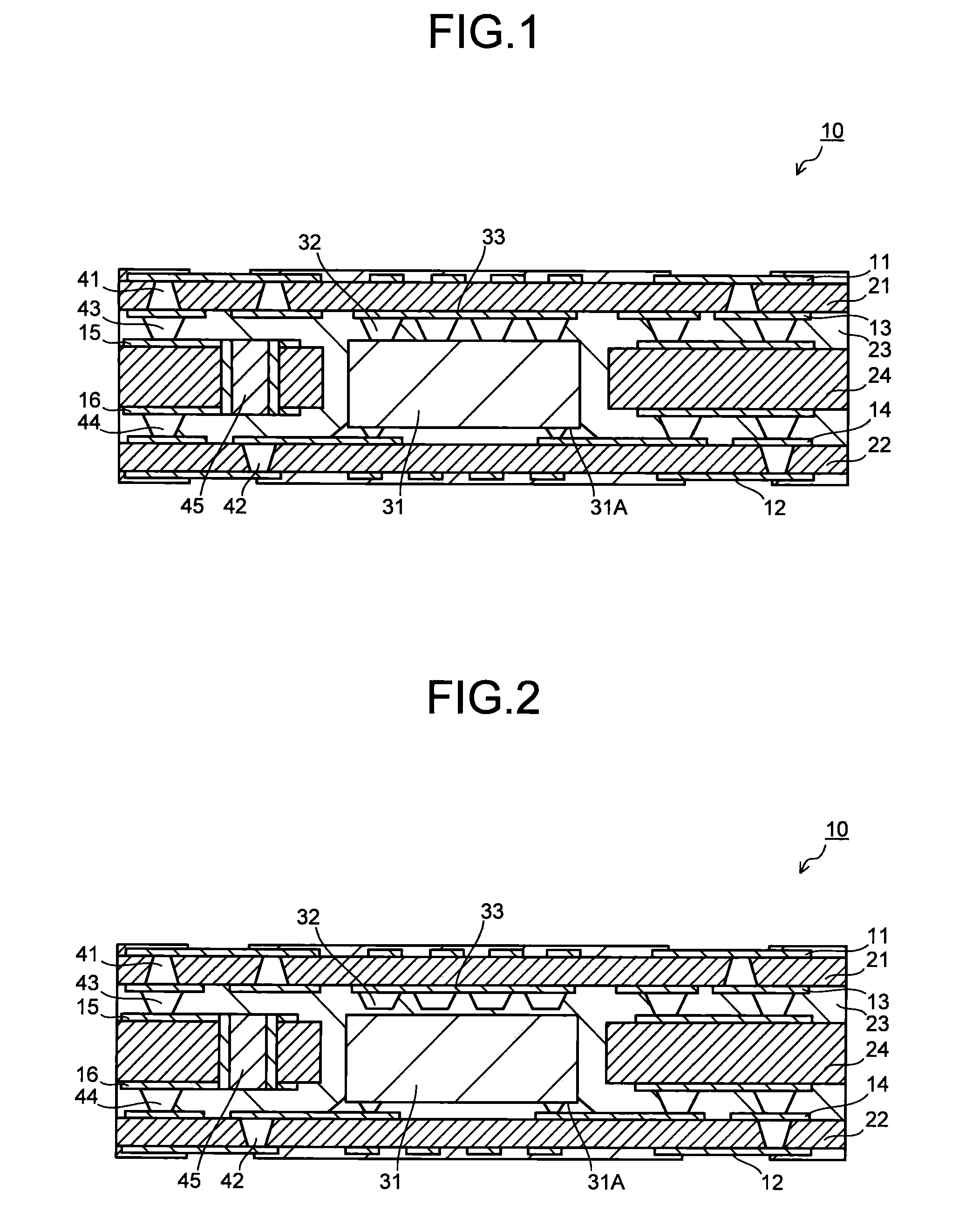
[0058]FIG. 3 is a cross sectional view showing the structure of an electronic component built-in wiring board according to a second embodiment. Like or corresponding components are designated by the same reference numerals through the drawings.

[0059]The electronic component built-in wiring board 10 in this embodiment is similar to the one in the first embodiment except that an additional metallic heat radiation plate 35 is provided on the first insulating layer 21 at the same surface level as the first wiring pattern 11, and an additional metallic bodies 34, which penetrates through the first insulating layer 21 and are connected with the metallic plates, 33, 35, is provided.

[0060]In the electronic component built-in wiring board 10 shown in FIG. 3, the metallic bodies 32 and 34 are connected with one another via the metallic plate 33, and the metallic bodies 34 are connected with the metallic plate 35 which is formed on the outermost surface of the wiring board 10. Therefore, the h...

third embodiment

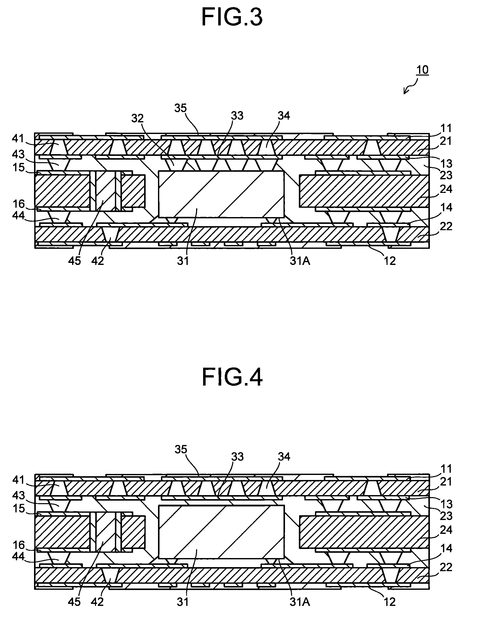
[0069]FIG. 5 is a cross sectional view showing the structure of an electronic component built-in wiring board according to a third embodiment. Like or corresponding components are designated by the same reference numerals through the drawings.

[0070]In the electronic component built-in wiring board 10 in this embodiment, the additional metallic heat radiation plate 35 is provided on the first insulating layer 21 at the same surface level as the first wiring pattern 11 and the additional metallic bodies 34 are provided which is formed through the first insulating layer 21 and connected with the metallic heat radiation plates 33 and 35. Moreover, a heat sink 37 is provided as a heat radiation member so as to be contacted with the metallic heat radiation plate 35.

[0071]In this embodiment, the metallic bodies 32 are connected with the metallic bodies 34 via the metallic plate 33 and the metallic bodies 34 are connected with the metallic plate 35 formed on the outermost surface of the wir...


PUM

PropertyMeasurementUnit
Thicknessaaaaaaaaaa
Electrical conductoraaaaaaaaaa
Metallic bondaaaaaaaaaa

Abstract

An electronic component built-in wiring board includes: at least a pair of wiring patterns; an insulating layer disposed between the pair of wiring board; an electronic component embedded in the insulating layer; and a metallic body provided at least on or above a main surface of the electronic component in the insulating layer and thermally contacted with the electronic component.

Description

CROSS-REFERENCE TO RELATED APPLICATIONS[0001]This application is based upon and claims the benefit of priorities from the prior Japanese Patent Application No. 2006-339689 filed on Dec. 18, 2006 and Japanese Patent Application No. 2007-319474 filed on Dec. 11, 2007; the entire contents which are incorporated herein by reference.BACKGROUND[0002]1. Field of the Invention[0003]The present invention relates to an electronic component built-in wiring board which can radiate heat generated at the electronic component thereof and a method for radiating the heat generated at the electronic component thereof. The electronic component built-in wiring board is configured such that the electronic component is embedded in an insulating member thereof.[0004]2. Background of the Invention[0005]Recently, with the development and downsizing of an electronic device, it is required to increase the arrangement density of circuit components and to develop the performances of the circuit components. In t...

Claims


Application Information

Patent Timeline
IPC IPC(8): H05K7/20H05K1/16H01S4/00
CPCH01L2224/16225H01L2224/73204H05K1/0206H05K1/186H05K3/4069H05K3/4614Y10T29/49002H05K3/4647H05K2201/09527H05K2201/096H05K2203/061H05K2203/063H05K3/462H01L2924/00014H01L2924/00011H01L2224/0401H05K1/18
Inventor SASAOKA, KENJIFUKUOKA, YOSHITAKA
Owner DAI NIPPON PRINTING CO LTD
Why Eureka
Try Eureka