Optical pixel and image sensor

Active Publication Date: 2010-02-04
BEN GURION UNIVERSITY OF THE NEGEV
View PDF7 Cites 49 Cited by
  • Summary
  • Abstract
  • Description
  • Claims
  • Application Information

AI Technical Summary

Benefits of technology

[0016]Some of the present embodiments are based on a multisampling dynamic range expansion approach, a

Problems solved by technology

The dynamic range problem exists when trying to capture scenes having a wide range of illumination.
Dynamic range insufficiency of conventional video cameras is a serious pro

Method used


Image

  • Optical pixel and image sensor
  • Optical pixel and image sensor
  • Optical pixel and image sensor

Examples


examples

[0155]Reference is now made to the following examples, which together with the above descriptions, illustrate the invention in a non-limiting fashion.

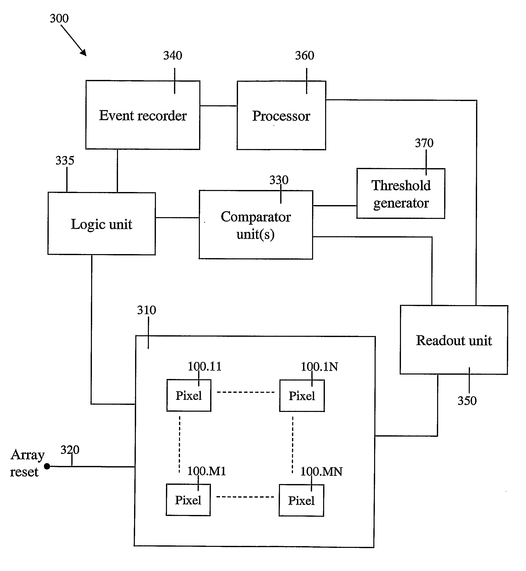
[0156]Reference is now made to FIG. 1, which is a simplified schematic diagram of an exemplary single pixel 1110, its corresponding processing circuitry 1120 and external digital memory 1130. Note, that both processing circuit 1120 and pixel 1110 may be designed in different ways, while still implementing the described algorithm.

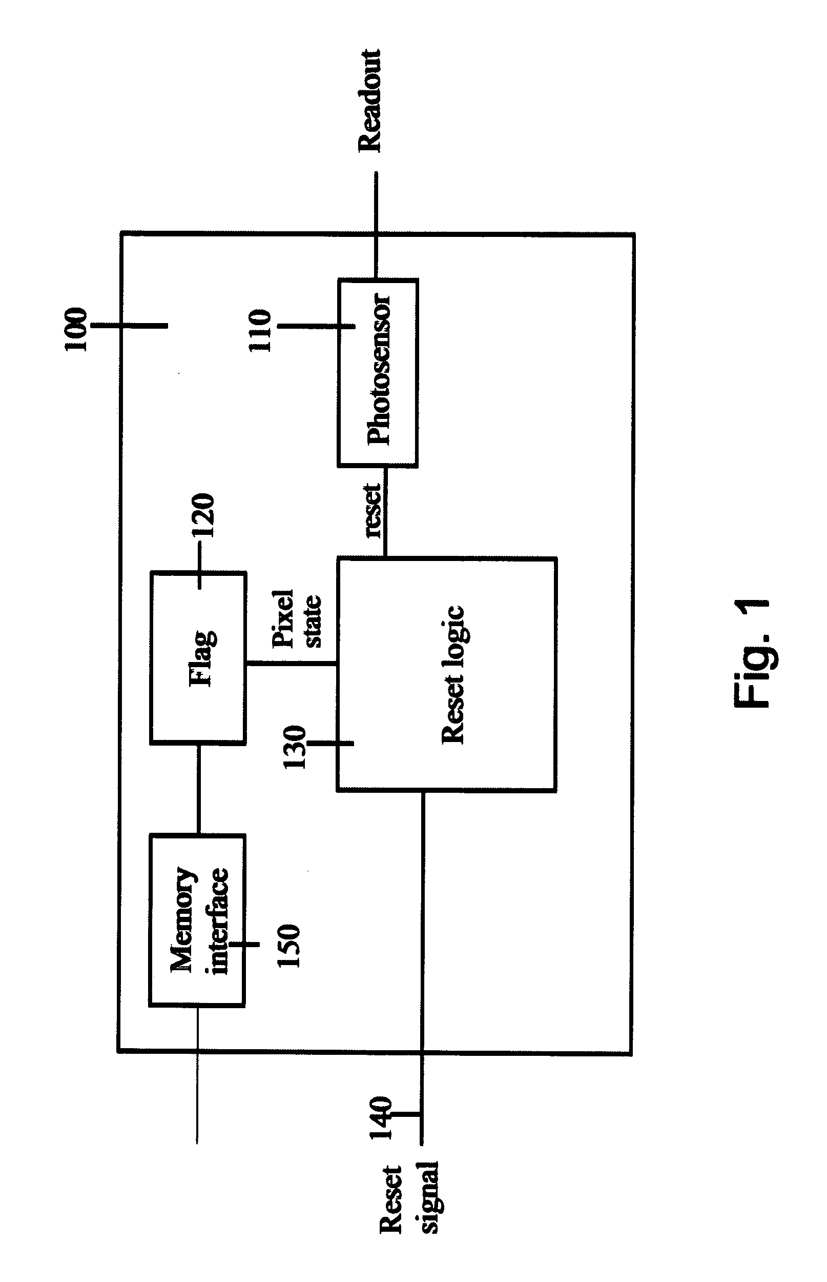
[0157]Pixel 1110 includes: (1) Photodiode, (2) Photodiode Reset switch, controlled by AND gate output, (3) Shutter switch, (4) 1-bit in-pixel digital memory for storing the flag (both static and dynamic memories may be implemented), (5) Analog buffer for analog signal readout, (6) Row Select switch, (7) AND gate to control locally reset operation of the pixel and (6) FD_Reset switch, used to reset the floating diffusion capacitance CFD. Exemplary pixel configurations are presented in FIGS. 13a and 13b.

[0158]Pr...


PUM


Abstract

A photosensitive pixel includes a photosensor and an externally loadable flag. The photosensor outputs a signal indicative of an intensity of incident light. The externally loadable flag indicates the pixel reset state, and is preferably stored in an in-pixel memory. Pixel reset logic resets the photosensor in accordance with the reset state and an externally applied reset signal.

Description

FIELD AND BACKGROUND OF THE INVENTION[0001]The present embodiments, in some embodiments thereof, relate to an image sensor based on pixels with reset state information, and more particularly, but not exclusively, to a method for selectively adjusting the integration time of each pixel, while permitting image sensor operation in global shutter mode.[0002]Driven by the demand for low-power dissipation in state-of-the-art portable image systems, CMOS Active Pixel Sensors (APS) have become very attractive. CMOS imagers offer significant advantages in terms of low-power, low-voltage and monolithic integration, thus rivaling traditional charge-coupled devices (1-3).[0003]Sensor dynamic range (DR) is one of the most important figures of merit in state of the art CMOS image sensors. The dynamic range problem exists when trying to capture scenes having a wide range of illumination. Generally, the illumination levels can range from 10−3 lux for night vision to 105 lux for scenes illuminated w...

Claims


Application Information

Patent Timeline
IPC IPC(8): H04N5/235H04N5/335
CPCH04N5/35536H04N3/155H04N25/58
Inventor BELENKY, ALEXANDERFISH, ALEXANDERYADID-PECHT, ORLY
Owner BEN GURION UNIVERSITY OF THE NEGEV
Why Eureka
Try Eureka