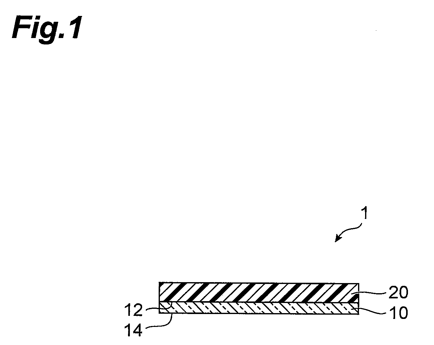
Photosensitive element
- Summary
- Abstract
- Description
- Claims
- Application Information
AI Technical Summary
Benefits of technology
Problems solved by technology
Method used
Image

Examples
example 1
[0116]A polyethylene terephthalate (hereinafter, “PET”) film (trade name: “A-1517” by Toyobo, Ltd., thickness: 16 μm) was prepared as a support film. The PET film was coated with the prepared photosensitive resin composition containing the binder polymer (I) to a uniform thickness and dried for 2 minutes with a hot air convection current drier at 100° C. to remove the solvent and form a photosensitive layer. After drying, the photosensitive layer was covered with a polyethylene film (trade name: “NF-15” by Tamapoly Co., Ltd., thickness: 20 μm) as a protective film to obtain a photosensitive element. The post-drying thickness of the photosensitive layer was 25 μm.
example 2
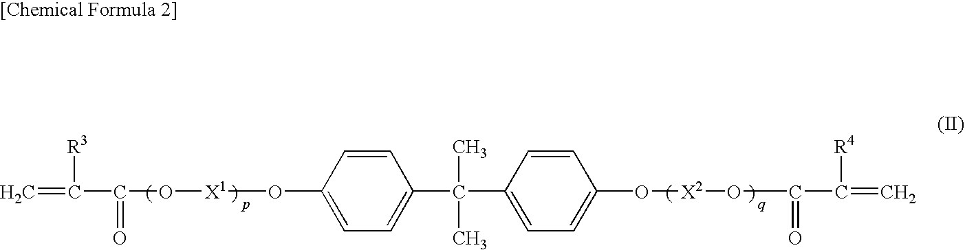
[0117]A photosensitive element was obtained in the same manner as Example 1, except that a photosensitive resin composition containing binder polymer (II) was used instead of binder polymer (I). The post-drying thickness of the photosensitive layer was 25 μm.
PUM
 Abstract
Description
Claims
Application Information
 - Generate Ideas
- Intellectual Property
- Life Sciences
- Materials
- Tech Scout
- Unparalleled Data Quality
- Higher Quality Content
- 60% Fewer Hallucinations
Browse by: Latest US Patents, China's latest patents, Technical Efficacy Thesaurus, Application Domain, Technology Topic, Popular Technical Reports.
© 2025 PatSnap. All rights reserved.Legal|Privacy policy|Modern Slavery Act Transparency Statement|Sitemap|About US| Contact US: help@patsnap.com