Mono-silicon solar cells

a solar cell and monosilicon technology, applied in the field of photovoltaics (pv) technology, can solve the problems of shortening the lifetime of electrons, and limiting the energy conversion efficiency of mono-silicon solar cells made from b-doped p-type substrates in massive production

Inactive Publication Date: 2010-02-04
E CUBE ENERGY TECH CO LTD
View PDF7 Cites 54 Cited by
  • Summary
  • Abstract
  • Description
  • Claims
  • Application Information

AI Technical Summary

Problems solved by technology

The energy conversion efficiency of mono-Si solar cells made from B-doped p-type substrates in massive production is typically limited to around 16-17% due to various loss mechanisms.
One loss mechanism is due to the recombination of the photo-generated carriers caused by defects and impurities that adversely shorten the lifetime of the minority carriers in the p-type absorber region, in addition to the non-radiative recombination in he heavily doped n-type region and at its surface.
Solar cells made from the B-doped substrates generally exhibit a certain degree of degradation after subjecting to strong photo-illumination presumably caused by high concentration oxygen impurity interacting with B dopants, shortening the lifetime of electrons and therefore limiting the conversion efficiency.
However, it is well known that Ga-doped single-crystal Si ingots grown by CZ method have very poor doping distribution uniformity in both axial and radial directions primarily due to the very small equilibrium segregation coefficient for Ga dopant in Si.
The small equilibrium segregation coefficient for Ga dopant in Si crystal growth inherently poses a great challenge to the industry as how to obtain a uniform doping distribution throughout the entire CZ growth process.
Even with controlling pull rate and rotation speed during the growth, large variation in resistivity from wafer to wafer resulting from non-uniform Ga doping distribution in Si ingots is still inevitable.
Recombination in the heavily doped diffusion region and at its surface is another major loss channel that impacts the conversion efficiency of mono-Si solar cells.
Addition of a surface passivation film, such as oxide, usually reduces the recombination at the surface, only partially resolving the problem.
Another loss mechanism in energy conversation efficiency is the shadowing effect of the front contact fingers.
So far, full backside contacted solar cells have only been successfully developed using n-type mono-Si.
Unfortunately, the vastly available and the most used CZ grown B-doped p-type Si single crystal wafers were found to consistently exhibit a not-so-well-understood degrading behavior in the lifetime of minority carriers (electrons) after subjecting to strong photo-illumination, preventing cells fabricated using B-doped wafers from achieving high conversion efficiency.
The consensus to the problem is that the phenomenon is most likely to be caused by the interaction of B dopants with oxygen impurity that were incorporated into the Si crystal during CZ growth, presumably forming B-O complex, resulting in the degradation of the effective lifetime of minority carriers and therefore limiting the cells' conversion efficiency.

Method used


Image

  • Mono-silicon solar cells
  • Mono-silicon solar cells
  • Mono-silicon solar cells

Examples


Embodiment Construction

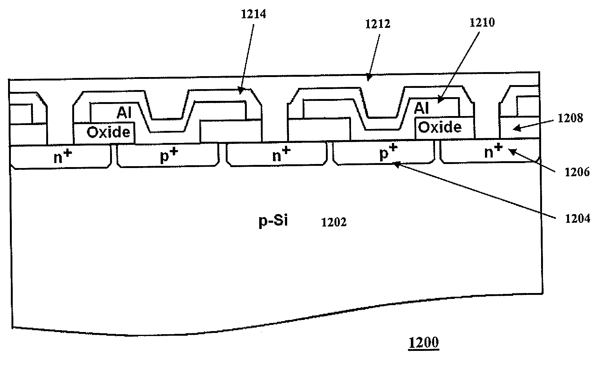
[0020]Disclosed herein are schemes designed to achieve maximum solar conversion efficiency for electricity power extraction from solar cells made from mono-Si substrates.

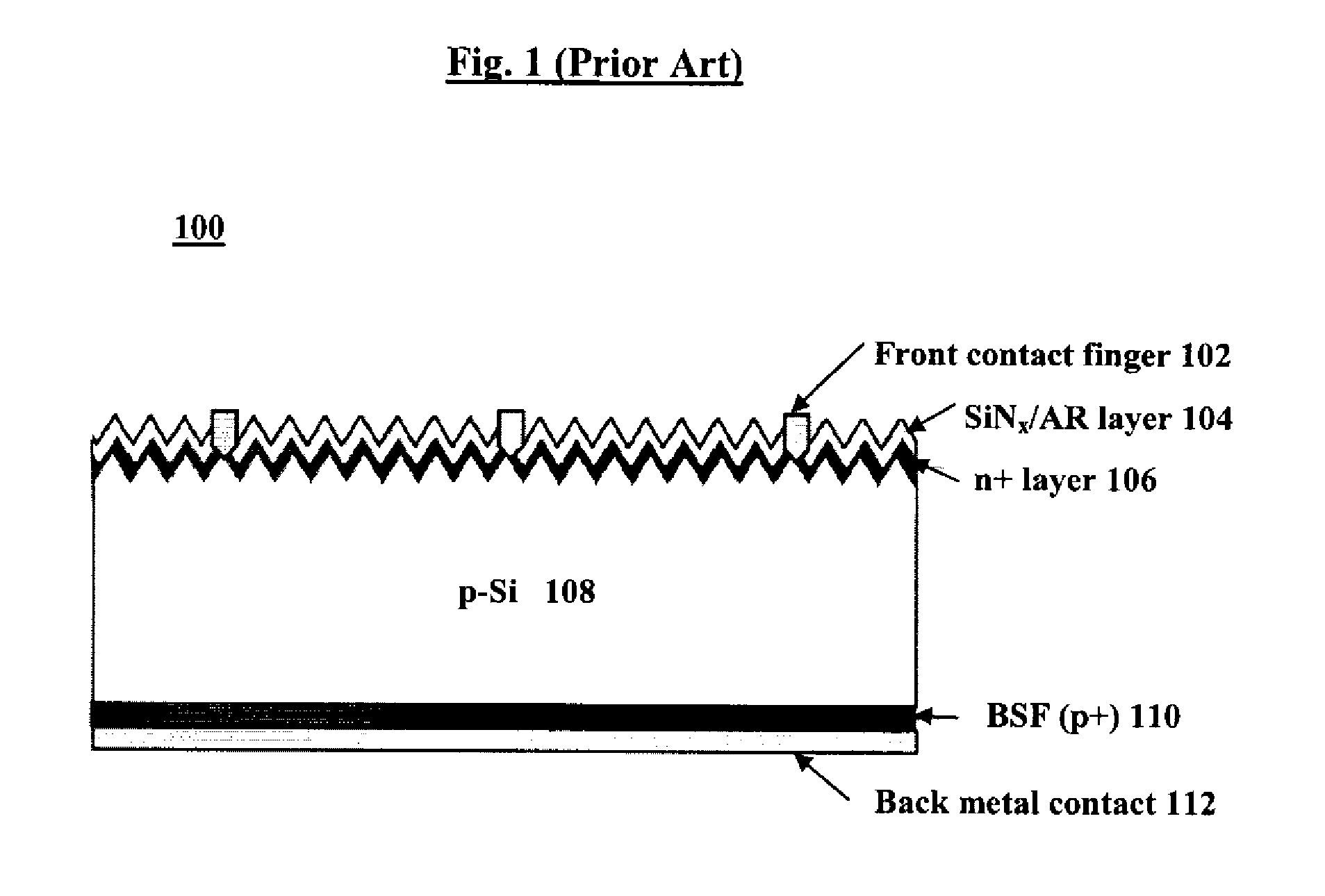
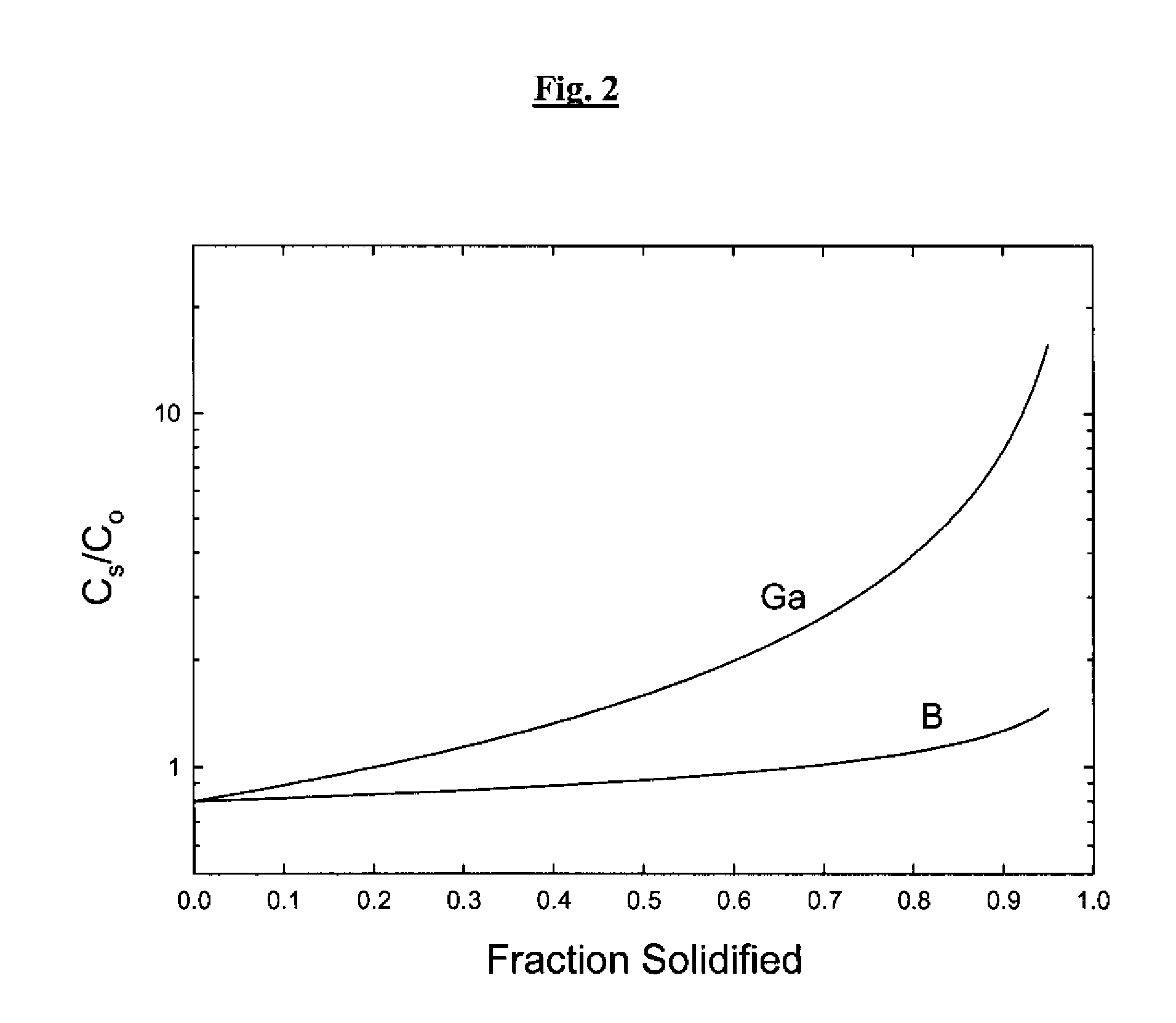
[0021]To improve conversion efficiency of mono-Si solar cells made from p-type substrates, Ga-doped rather than B-doped wafers are used in order to suppress the influence of high concentration oxygen impurity, which is ubiquitous in CZ grown single-crystal Si ingots, on the performance of the solar cells. To obtain p-type mono-Si wafers doped by Ga, it is necessary to grow p-type single-crystal Si ingots with resistivity ranging from 0.1 to 10 Ω-cm using Czochralski method. Ga-doped melt sources may be prepared by mixing Ga dopant at concentrations of approximately from 1×10¹⁷ to 2×10¹⁹ atoms / cm3 with Si. However, as previously mentioned, achieving uniform distributed doping concentration in Ga-doped Si ingots pulling by CZ method is very difficult. As a result, a small amount of B at a ratio less than one atomic pe...


PUM


Abstract

A method for producing a backside contact of a single p-n junction photovoltaic solar cell is provided. The method includes the steps of: providing a p-type substrate having a back surface; providing a plurality of p+ diffusion regions at the back surface of the substrate; providing a plurality of n+ diffusion regions at the back surface of the substrate in an alternate pattern with the p+ diffusion regions; providing an oxide layer over the p+ and n+ regions; providing an insulating layer over the back surface of the substrate; providing at least one first metal contact at the back surface for the p+ diffusion regions; and providing at least one second metal contact at the back surface for the n+ diffusion regions.

Description

CROSS-REFERENCE TO RELATED APPLICATIONS[0001]This application claims priority to U.S. Provisional Patent Application Ser. Nos. 60 / 981,108 filed Oct. 18, 2007, 60 / 985,624 filed Nov. 5, 2007, and 60 / 985,627 filed Nov. 5, 2007, the contents of all of which are incorporated herein by reference.FIELD OF THE INVENTION[0002]The present invention relates to the field of photovoltaics (PV) technology that converts solar energy directly into electrical energy. More particularly, the present invention relates to optimizing material parameters of single-crystal silicon (mono-Si) wafers that are used to fabricate PV solar cells, as well as device structures of the solar cells in order to achieve maximum solar energy conversion efficiency, extracting more power of electricity from available solar irradiance.BACKGROUND OF THE INVENTION[0003]PV is a technology typically using large area p-n junction diodes to convert sunlight into electricity. These p-n junction diodes are therefore called solar ce...

Claims


Application Information

Patent Timeline
Patent Type & Authority Applications(United States)
IPC IPC(8): H01L21/768
CPCH01L31/022425H01L31/068Y02E10/547H01L31/022441H01L31/0682H01L31/1804Y02P70/50
Inventor SHAN, WEIXIANG, XIAO-DONG
Owner E CUBE ENERGY TECH CO LTD
Why Eureka
Try Eureka