

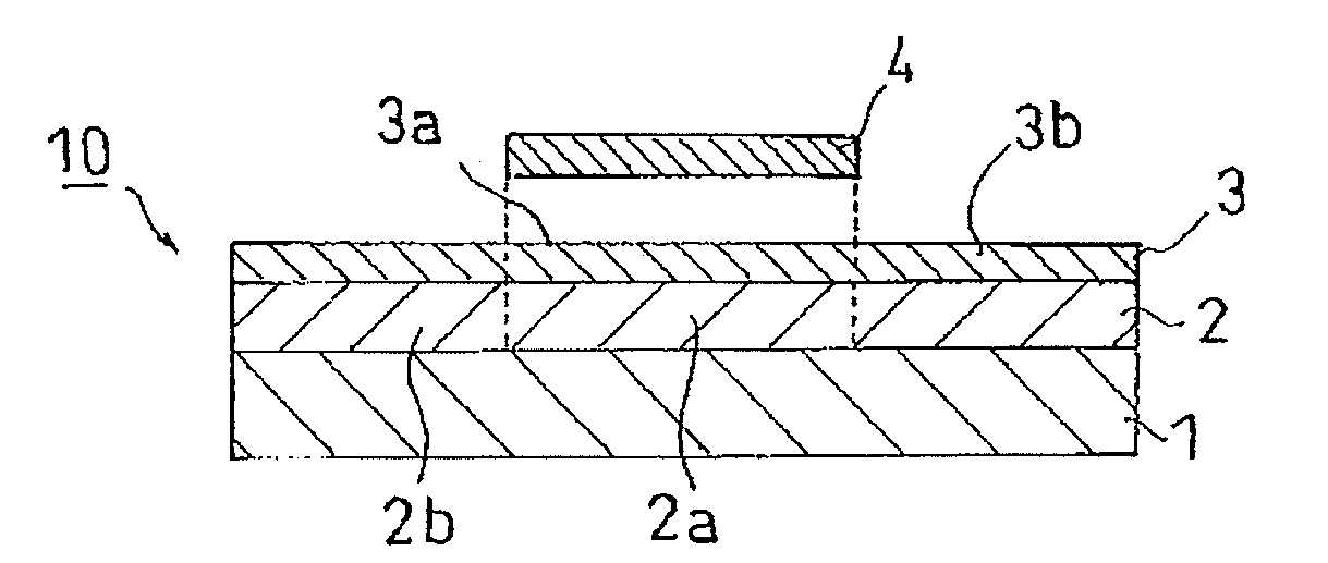
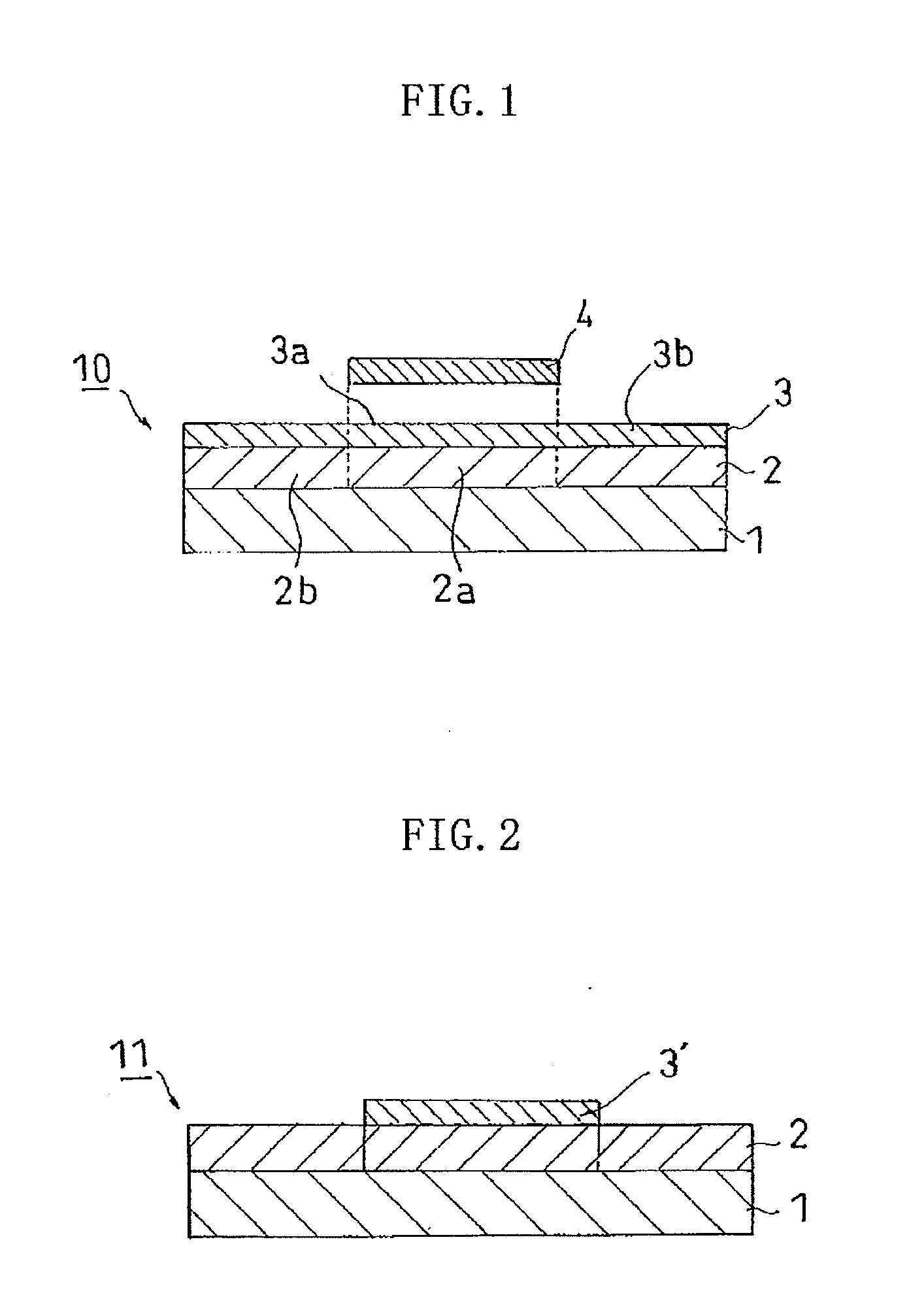
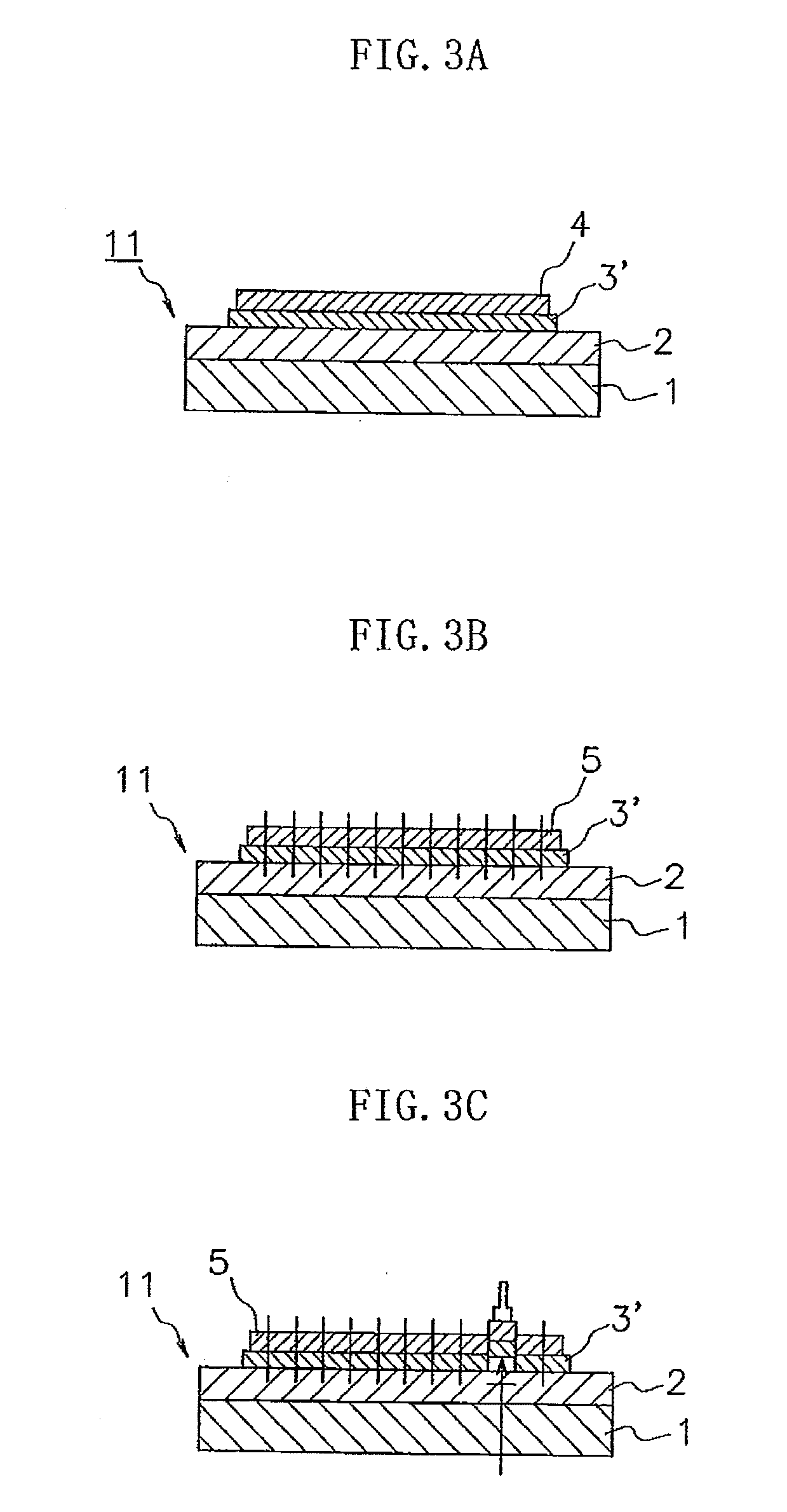
Dicing die-bonding film
- Summary
- Abstract
- Description
- Claims
- Application Information
AI Technical Summary
Benefits of technology
Problems solved by technology
Method used
Image

Examples
example 1
Production of Dicing Film
[0103]Acrylic polymer A having a weight average molecular weight of 580,000 was obtained by placing 51.7 parts of 2-ethylhexyl acrylate (hereinafter referred to as “2EHA”), 39.0 parts of stearyl acrylate (hereinafter referred to as “SA”), 9.3 parts of 2-hydroxyethyl acrylate (below, referred to as “HEA”), 0.2 parts of benzoyl peroxide, and 65 parts of toluene into a reactor equipped with a cooling tube, a nitrogen-introducing tube, a thermometer, and a stirring apparatus, and performing a polymerization treatment at 61° C. in a nitrogen airflow for 6 hours. The weight average molecular weight is as follows. The molar ratio of 2EHA to SA to HEA was made to be 70 mol:30 mol:20 mol.
[0104]An acrylic polymer A′ was obtained by adding 10.0 parts (80 mol % to HEA) of 2-methacryloyloxyethyl isocyanate (in the following, referred to as “MOI”) into this acrylic polymer A and performing an addition reaction treatment at 50° C. in an air flow for 48 hours.
[0105]Next, a ...
examples 2 to 13
[0126]In each of Examples 2 to 13, the dicing die-bonding film was produced in the same manner as in Example 1 except that the composition and the compounded ratio were changed to those shown in Table 1.
TABLE 1HYDROXYLGROUP-ACRYLICACRYLICCONTAININGISOCYANATEESTER AESTER BMONOMERCOMPOUNDPHOTOPOLYMERIZATION2EHAi-OASAVABAHEA4HBAMOIAOITOLUENEC / LINITIATOREXAMPLE 151.7—39.0—— 9.3—10.06585(70) (30) (20) (80) EXAMPLE 253.7—40.5—— 5.8— 6.4—6585(70) (30) (12) (83) EXAMPLE 349.4—37.3——13.3—14.3—6585(70) (30) (30) (80) EXAMPLE 468.5—44.3——10.2—10.9—6585(85) (35) (20) (80) EXAMPLE 546.7—39.0—— 9.1— 9.7—6585(65) (30) (20) (80) EXAMPLE 6—51.738.2—— 9.3—10.0—6585(70) (30) (20) (80) EXAMPLE 750.6—38.2———11.3 9.7—6585(70) (30) (20) (80) EXAMPLE 851.7—39.0—— 9.3—— 9.16585(70) (30) (20) (80)EXAMPLE 951.7—39.0—— 9.3— 8.7—6585(70) (30) (20) (70) EXAMPLE51.7—39.0—— 9.3—11.2—658510(70) (30) (20) (90) EXAMPLE51.7—39.0—— 9.3—10.0—1008511(70) (30) (20) (80) EXAMPLE5...
PUM
| Property | Measurement | Unit |
|---|---|---|
| Temperature | aaaaa | aaaaa |
| Tensile modulus | aaaaa | aaaaa |
| Fraction | aaaaa | aaaaa |
Abstract
Description
Claims
Application Information