

Dicing die-bonding film
- Summary
- Abstract
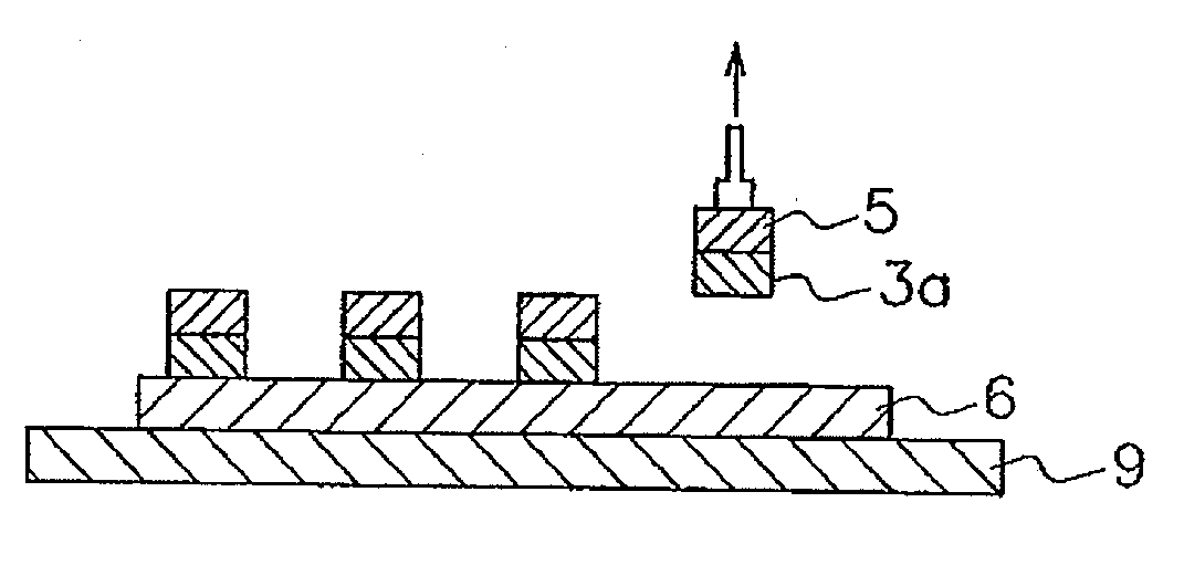
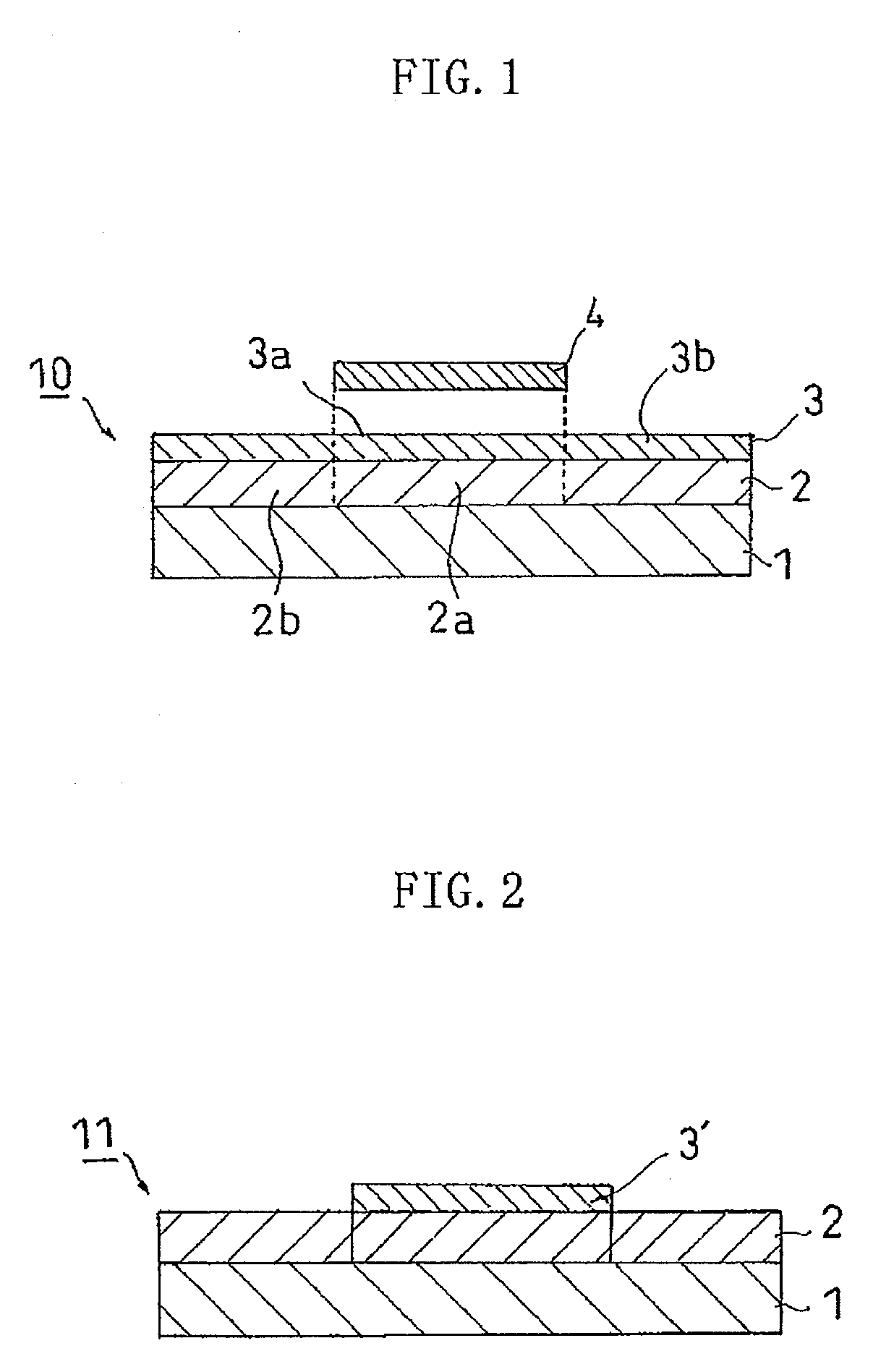
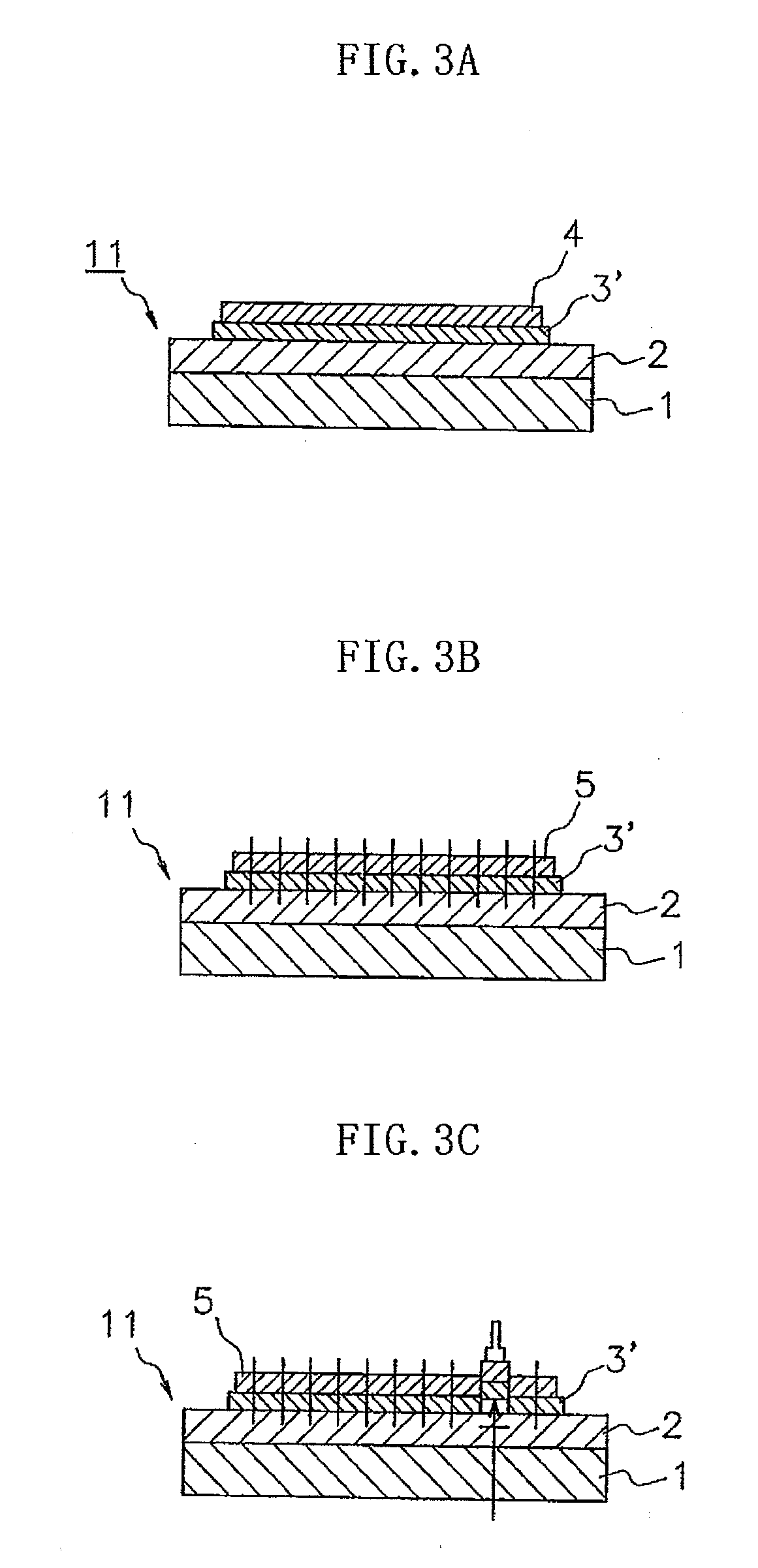
- Description
- Claims
- Application Information
AI Technical Summary
Benefits of technology
Problems solved by technology
Method used
Image

Examples
examples 1
Production of Dicing Film
[0106]An acrylic polymer A having a weight average molecular weight of 850,000 was obtained by placing 88.8 parts of 2-ethylhexylacrylate (in the following, referred to as “2EHA”), 11.2 parts of 2-hydroxyethylacrylate (in the following, referred to as “HEA”), 0.2 parts of benzoyl peroxide, and 65 parts of toluene in a reactor equipped with a cooling tube, a nitrogen-introducing tube, a thermometer, and a stirring apparatus, and performing a polymerization treatment at 61° C. in a nitrogen airflow for 6 hours. The weight average molecular weight is as follows. The molar ratio of 2EHA to HEA was made to be 100 mol:20 mol.
[0107]An acrylic polymer A′ was obtained by adding 12 parts (80 mol % to HEA) of 2-methacryloyloxyethyl isocyanate (in the following, referred to as “MOI”) into this acrylic polymer A and performing an addition reaction treatment at 50° C. in an air flow for 48 hours.
[0108]Next, a pressure-sensitive adhesive solution was produced by adding 8 p...
examples 2 to 14
[0131]In each of Examples 2 to 14, a dicing die-bonding film was produced in the same manner as Example 1 except that the composition and the compounded ratio were changed to those shown in Table 1.
example 15
[0132]In the present example, a dicing die-bonding film was produced in the same manner as Example 1 except that the standing step after transferring the die-bonding film to the pressure-sensitive adhesive layer precursor of the dicing die-bonding film was performed under an environment of a temperature at 25±3° C. and a relative humidity at 85% or less for 12 hours.
PUM
| Property | Measurement | Unit |
|---|---|---|
| Temperature | aaaaa | aaaaa |
| Tensile modulus | aaaaa | aaaaa |
| Fraction | aaaaa | aaaaa |
Abstract
Description
Claims
Application Information