Method and system for facilitating floorplanning for 3D IC

a three-dimensional, floor-planning technology, applied in multi-objective optimization, instruments, cad techniques, etc., can solve the problems of reducing the area efficiency to about 30%, a true system-on-a-chip device with a large variety of functional circuit blocks, e.g. logic, analog and memory, etc., to achieve the effect of improving the efficiency of the floor-planning area

Active Publication Date: 2010-02-04
SYNOPSYS INC
View PDF7 Cites 216 Cited by
  • Summary
  • Abstract
  • Description
  • Claims
  • Application Information

AI Technical Summary

Benefits of technology

[0018]In a further variation, the system increases the time-varying parameter after the time-varying parameter reaches the pre-determined intermediate value, thereby allowing the decomposed blocks to experience additional perturbation.

Problems solved by technology

The die-to-package ratio is generally low (on the order of 50%) and additional spacing between components on the board is typically required, which further reduces the area efficiency to about 30%.
A true system-on-a-chip (SOC) device with a large variety of functional circuit blocks, e.g., logic, analog, and memory, is fairly difficult to build.
Because 3D ICs tend to be more complex since they integrate larger amounts of functionality and contain diverse technologies, the design, representation, and optimization of 3D ICs require changes to many stages in the design flow.
Furthermore, it will be necessary to represent constraints imposed by multiple technologies concurrently.
Certain problems, such as heat dissipation, which are already becoming an issue for 2D ICs, will gain greater prominence with 3D ICs.
This challenge is due to the larger power density in the 3D structure and the poor thermal conductivity of the dielectric layers between the device layers, which can increase the possibility of thermal runaway of the chip.
These techniques do not consider manufacturability and design constraints, and often appear inadequate in obtaining a global optimized solution.

Method used


Image

  • Method and system for facilitating floorplanning for 3D IC
  • Method and system for facilitating floorplanning for 3D IC
  • Method and system for facilitating floorplanning for 3D IC

Examples


Embodiment Construction

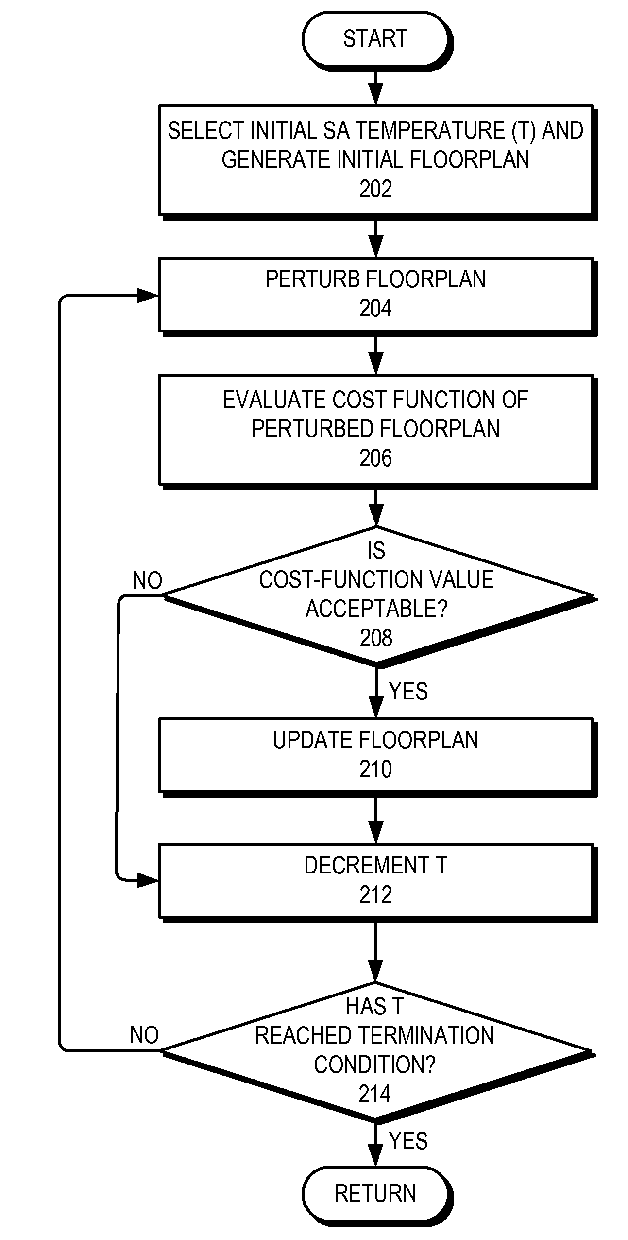
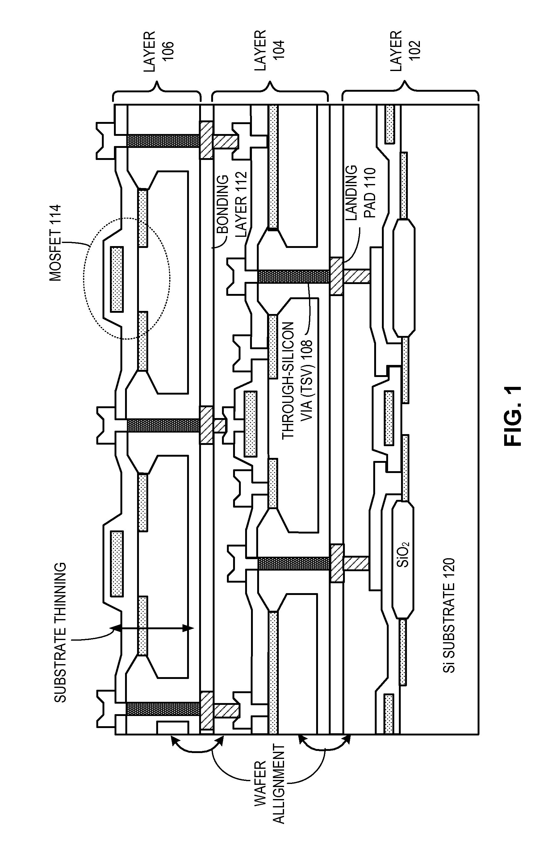
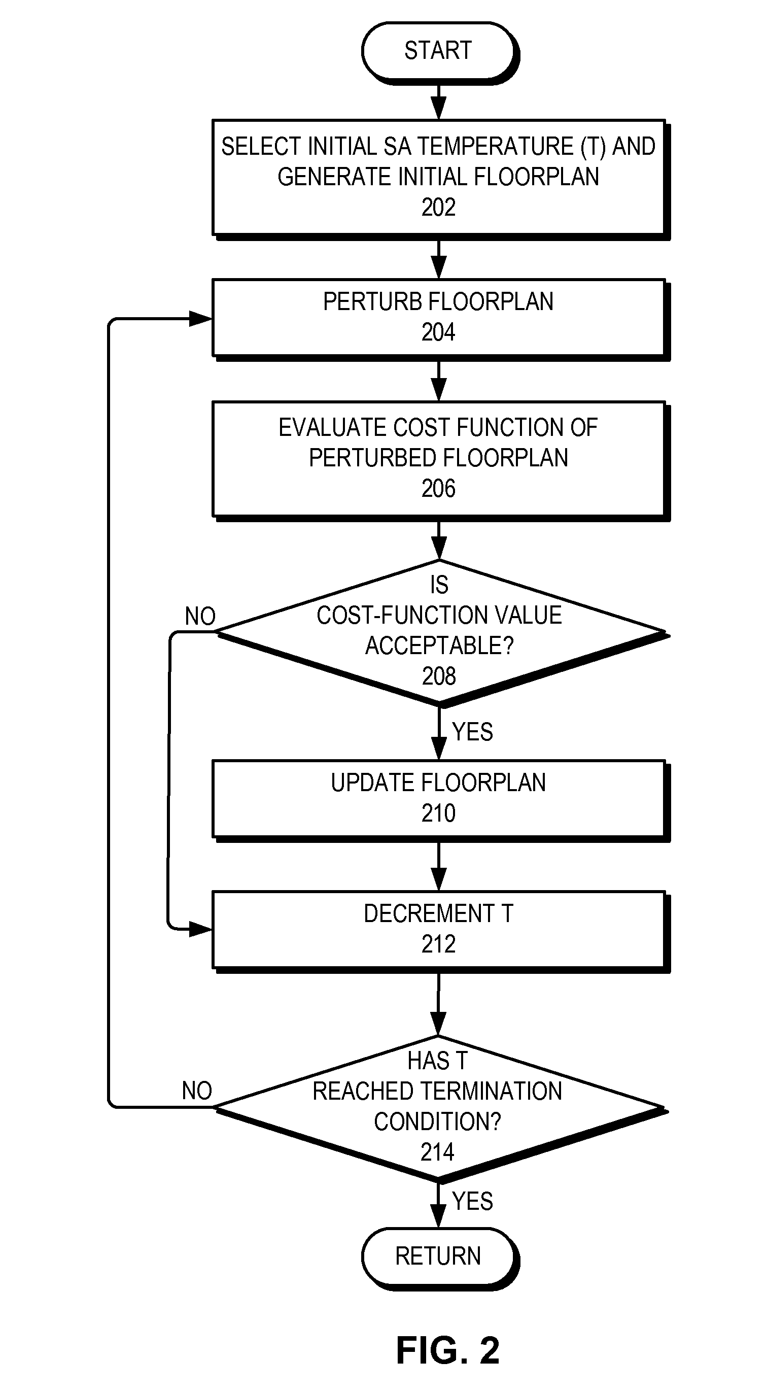
[0027]The following description is presented to enable any person skilled in the art to make and use the invention, and is provided in the context of a particular application and its requirements. Various modifications to the disclosed embodiments will be readily apparent to those skilled in the art, and the general principles defined herein may be applied to other embodiments and applications without departing from the spirit and scope of the present invention. Thus, the present invention is not limited to the embodiments shown, but is to be accorded the widest scope consistent with the principles and features disclosed herein.

[0028]The data structures and code described in this detailed description are typically stored on a computer-readable storage medium, which may be any device or medium that can store code and / or data for use by a computer system. The computer-readable storage medium includes, but is not limited to, volatile memory, non-volatile memory, magnetic and optical st...


PUM


Abstract

One embodiment of the present invention provides a system for facilitating floorplanning for three-dimensional integrated circuits (3D ICs). During operation, the system receives a number of circuit blocks. The system places the blocks in at least one layer of a multi-layer die structure and sets an initial value of a time-varying parameter. The system then iteratively perturbs the block arrangement until the time-varying parameter reaches a pre-determined value.

Description

FIELD [0001]The present disclosure relates generally to the design of integrated circuits (ICs). More specifically, the present disclosure relates to a method and system for facilitating floorplanning in three-dimensional (3D) ICs.RELATED ART [0002]The continued shrinking of very-large-scale integration (VLSI) circuits according to the Moore's Law mandates packaging and interconnection technologies to keep up. Three-dimensional integrated circuits (3D ICs) are gaining much interest as a viable solution to help maintain the pace of system demands on scaling, performance, and functionality.[0003]A key benefit of 3D ICs is system-size reduction. In traditional technologies, system assembly is based on two-dimensional (2D) planar architecture. Dies are individually packaged and connected on a planar interconnect substrate, e.g., printed circuit boards (PCBs). The die-to-package ratio is generally low (on the order of 50%) and additional spacing between components on the board is typical...

Claims


Application Information

Patent Timeline
Patent Type & Authority Applications(United States)
IPC IPC(8): G06F17/50
CPCG06F17/504G06F2217/08G06F17/5072G06F30/3323G06F30/392G06F2111/06
Inventor SINHA, SUBARNAREKHACHIANG, CHARLES C.
Owner SYNOPSYS INC
Why Eureka
Try Eureka