Array substrate for in-plane switching mode liquid crystal display device and method of fabricating the same

a liquid crystal display and substrate technology, applied in non-linear optics, instruments, optics, etc., can solve problems such as deterioration of display image quality

Active Publication Date: 2010-02-11
LG DISPLAY CO LTD
View PDF4 Cites 35 Cited by
  • Summary
  • Abstract
  • Description
  • Claims
  • Application Information

AI Technical Summary

Benefits of technology

[0015]Accordingly, embodiments of the invention are directed to an array substrate for an in-plane switching (IPS) mode LCD device and a...

Problems solved by technology

As a result, there is a difference in a common voltage applied to the common elect...

Method used


Image

  • Array substrate for in-plane switching mode liquid crystal display device and method of fabricating the same
  • Array substrate for in-plane switching mode liquid crystal display device and method of fabricating the same
  • Array substrate for in-plane switching mode liquid crystal display device and method of fabricating the same

Examples


Embodiment Construction

[0031]Reference will now be made in detail to exemplary embodiments of the invention, which are illustrated in the accompanying drawings.

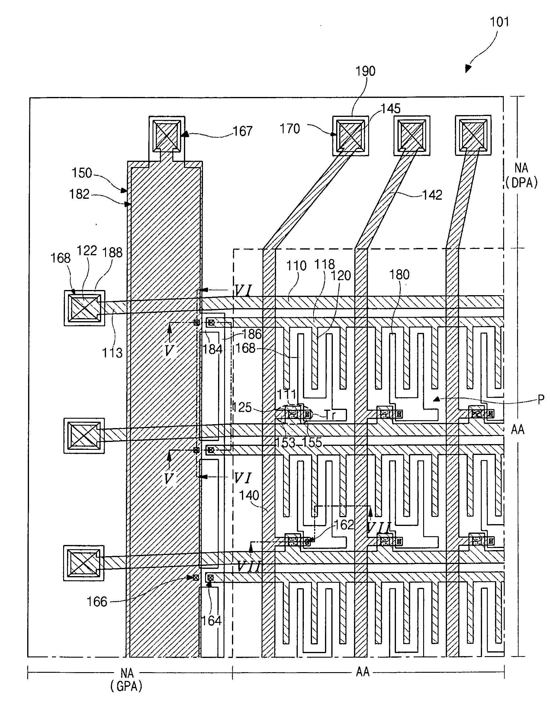
[0032]FIG. 4 is a schematic plan view of an array substrate for an IPS mode LCD device according to the present invention. In FIG. 4, a display region AA, where images are displayed, and a non-display region NA are defined in an array substrate 101. In the display region AA, gate and data lines 110 and 140 are formed. The gate and data lines 110 and 140 cross each other such that a pixel region P is defined. A common line 118 is formed to be parallel to the gate line 110. A thin film transistor (TFT) Tr connected to the gate and data lines 110 and 140 is formed in each pixel region P. The TFT Tr includes a gate electrode 111, gate insulating layer (not shown), a semiconductor layer 125 including an active layer (not shown) and an ohmic contact layer (not shown), a source electrode 153 and a drain electrode 155. In addition, a pixel electrode 180 co...


PUM


Abstract

An array substrate for an in-plane switching mode liquid crystal display device includes a plurality of gate lines on a substrate including a display region and a non-display region at a periphery of the display region; a plurality of common lines in the display region and parallel to the gate line, an end of each of the common lines disposed in the non-display region; a plurality of gate link lines each connected to an end of each of the gate lines and disposed in the non-display region; a gate insulating layer on the gate lines, the common lines and the gate link lines; a plurality of data lines on the gate insulating layer and crossing the gate lines to define a plurality of pixel regions in the display region; a first auxiliary common line on the gate insulating layer and in the non-display region, the first auxiliary common line crossing the gate link lines; a passivation layer on the data lines and the first auxiliary common line, the passivation layer including a first contact hole exposing the end of each of the common lines and a second contact hole exposing a portion of the first auxiliary common line; and a second auxiliary common line on the passivation layer and overlapping the first auxiliary common line, the second auxiliary common line electrically connected to the first auxiliary common line through the second contact hole and each of the common lines though the first contact hole, wherein the second auxiliary common line has substantially the same shape as the first auxiliary common line.

Description

[0001]The present invention claims the benefit of Korean Patent Application No. 10-2008-0077570 filed in Korea on Aug. 7, 2008, which is hereby incorporated by reference.BACKGROUND OF THE INVENTION[0002]1. Field of the Invention[0003]The invention relates to a liquid crystal display (LCD) device, and more particularly, to an array substrate for an in-plane switching (IPS) mode LCD device resolving a contact problem in a gate pad region and a method of fabricating the array substrate.[0004]2. Discussion of the Related Art[0005]Recently, as the society has entered in earnest upon an information age, there is a requirement in properties of a thin profile, light weight and low power consumption for a flat panel display.[0006]The flat panel display device is classified into an emission type and a non-emission type depending on whether the flat panel display device emits light or not. Since the emission type flat panel display device emits light, the emission type flat panel display devic...

Claims


Application Information

Patent Timeline
IPC IPC(8): G02F1/1343G02F1/13
CPCG02F1/134363G02F1/136286G02F1/1345G02F1/1343
Inventor LEE, YOUNG-HUN
Owner LG DISPLAY CO LTD
Why Eureka
Try Eureka