Optical waveguide and spot size converter using the same

a technology of optical waveguides and spot size converters, applied in the direction of optical waveguide light guides, instruments, optics, etc., can solve the problems of difficult to change difficult to adjust the mode diameter to the mode diameter of optical fibers, and high cost, and achieve high efficiency.

Active Publication Date: 2010-02-18
NEC CORP
View PDF3 Cites 85 Cited by
  • Summary
  • Abstract
  • Description
  • Claims
  • Application Information

AI Technical Summary

Benefits of technology

[0022]According to the present invention, when the optical waveguide is coupled with the optical fiber, coupling can be done in a highly efficient manner.

Problems solved by technology

However, changing the mode diameter of the optical fiber is difficult especially in the case of a multi-channel fiber array.
Even if it is possible, costs are extremely high.
Therefore, it is becoming difficult to adjust the mode diameter to that of the optical fiber.

Method used


Image

  • Optical waveguide and spot size converter using the same
  • Optical waveguide and spot size converter using the same
  • Optical waveguide and spot size converter using the same

Examples


example 1

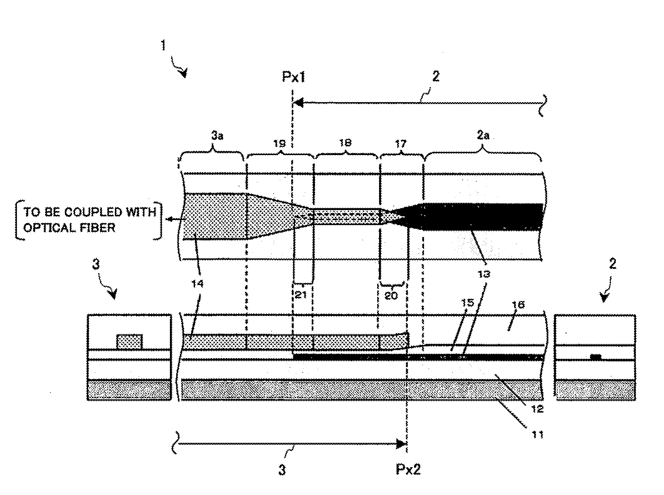
[0052]FIG. 1 is a schematic diagram which schematically illustrates an example of the configuration of a spot size converter that uses an optical waveguide 1 according to a first example of the present invention. FIG. 1A is a cross-sectional view of upper-surface essential components. FIG. 1B is a cross-sectional view of plain-surface essential components. FIG. 1C is a cross-sectional view of right-side-surface essential components. FIG. 1D is a cross-sectional view of left-side-surface essential components. Incidentally, FIGS. 1A and 1B show the cross-section surface of an essential portion of the optical waveguide 1. As indicated by undulating lines in the diagram, both ends of the optical waveguide 1 are not limited to the end faces of an actual waveguide chip. Moreover, in the case of the example illustrated by the diagram, the optical waveguide 1 is coupled with the optical fiber. Alternatively, the optical waveguide 1 may be applied in other cases, such as when the optical wav...

example 2

[0068]The following describes a second example of the present invention in detail with reference to the accompanying drawing.

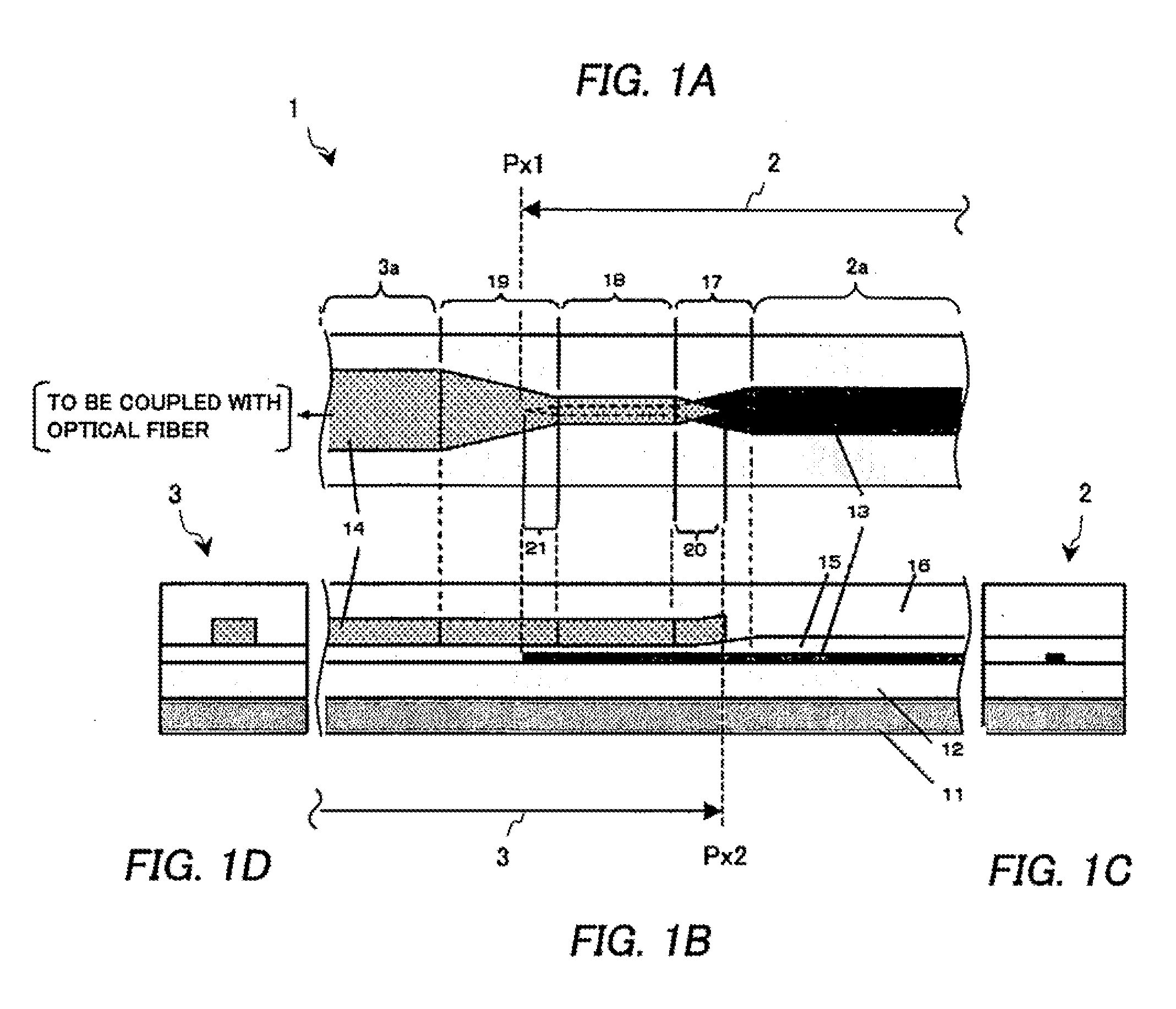
[0069]FIG. 2 is a schematic diagram which schematically illustrates an example of the configuration of an optical waveguide 1 according to the present example. FIG. 2A is a cross-sectional view of upper-surface essential components. FIG. 2B is a cross-sectional view of plain-surface essential components. FIG. 2C is a cross-sectional view of right-side-surface essential components. FIG. 2D is a cross-sectional view of left-side-surface essential components.

[0070]The optical waveguide 1 of the present example shown in FIGS. 2A to 2D has the same basic configuration as the optical waveguide of the first example has. However, the difference between the present example and the first example is that the optical waveguide 1 of the present example does not have the first reflection-free termination section 20 and the second reflection-free termination section 21. The ...

example 3

[0074]The following describes a third example of the present invention in detail with reference to the accompanying drawing.

[0075]FIG. 3 is a schematic diagram which schematically illustrates an example of the configuration of an optical waveguide according to the present example. FIG. 3A is a cross-sectional view of upper-surface essential components. FIG. 3B is a cross-sectional view of plain-surface essential components. FIG. 3C is a cross-sectional view of right-side-surface essential components. FIG. 3D is a cross-sectional view of left-side-surface essential components.

[0076]The optical waveguide 1 of the present example shown in FIGS. 3A to 3D has the same basic configuration as the optical waveguide of the first example has. However, the difference between the present example and the first example is that in the optical waveguide 1 of the present example, the mode conversion section 19 does not have a tapered portion. The following describes the difference.

[0077]The present ...


PUM


Abstract

An optical waveguide includes a substrate in the shape of a flat plate; lower clad that is disposed on the substrate; and a core that is disposed on the lower clad and transmits light. The optical waveguide includes a first optical waveguide and a second optical waveguide. The first optical waveguide includes a first core on the lower clad, and is disposed so as to extend along a direction in which the light travels to a first position. The second optical waveguide includes a second core on the lower clad, is disposed so as to extend along a direction in which the light travels to a second position, and has a lower relative refractive index difference than the first optical waveguide. The first optical waveguide and the second optical waveguide form, between the first position and the second position, a layer structure where the first core and the second core are disposed such that the first core is positioned a predetermined distance away from the second core in a direction perpendicular to the substrate. At least either the first optical waveguide or the second optical waveguide includes a mode coupling section and a mode conversion section. The mode coupling section includes a directional coupler to conduct the mode coupling of the first core and the second core between the first position and the second position. The mode conversion section is connected to the mode coupling section, and has a tapered core structure to adjust the mode diameter of the first core to the mode diameter of the second core.

Description

TECHNICAL FIELD[0001]The present invention relates to an optical waveguide and a spot size converter using the same, and particularly relates to the shape of the optical waveguide to be coupled with an optical fiber and an idea about the structure of the optical waveguide.BACKGROUND ART[0002]As communication technologies have advanced in recent years, various kinds of development have been conducted on an optical circuit which is part of an optical communication system. Since a planar lightwave circuit is excellent in terms of improving functions, downsizing and lowering costs, expectations are running high for an optical waveguide device.[0003]In the optical waveguide device, in order to couple the optical waveguide with the optical fiber in a highly efficient manner, the mode of the optical waveguide needs to match the mode of the optical fiber. In general, compared with the optical fiber, the relative refractive index difference Δ of the optical waveguide is large, and the mode d...

Claims


Application Information

Patent Timeline
Patent Type & Authority Applications(United States)
IPC IPC(8): G02B6/26G02B6/10
CPCG02B6/305G02B6/1228
Inventor DEKI, YUKARITAKAHASHI, MORIO
Owner NEC CORP
Why Eureka
Try Eureka