Usj techniques with helium-treated substrates

a technology of helium-treated substrates and helium-treated substrates, which is applied in the direction of antibacterial agents, electrical equipment, semiconductor devices, etc., can solve the problems of ms anneal being unable to completely remove the damage of the implant, the end of range damage, and the subsequent leakage of complementary metal oxide semiconductor (cmos) transistors, etc., to achieve the effect of lowering the resistance of the substrate and enhancing the activation

Active Publication Date: 2010-02-18
VARIAN SEMICON EQUIP ASSOC INC
View PDF13 Cites 14 Cited by
  • Summary
  • Abstract
  • Description
  • Claims
  • Application Information

AI Technical Summary

Benefits of technology

[0024]The problems of the prior art are addressed by the present disclosure, which describes a method of using helium to create ultra shallow junctions. A pre-implantation amorphization using helium has significant advantages. For example, it has been shown that upon anneal dopants will penetrate the substrate only to the original amorphous-crystalline interface, and no further. Therefore, by properly determining the implant energy of helium, it is possible to exa...

Problems solved by technology

This method may cause residual damage at the end of range and subsequent leakage in complementary metal oxide semiconductor (CMOS) transistors.
A MS anneal is unable to completely remove implant damage caused by silicon ...

Method used


Image

  • Usj techniques with helium-treated substrates
  • Usj techniques with helium-treated substrates
  • Usj techniques with helium-treated substrates

Examples


Embodiment Construction

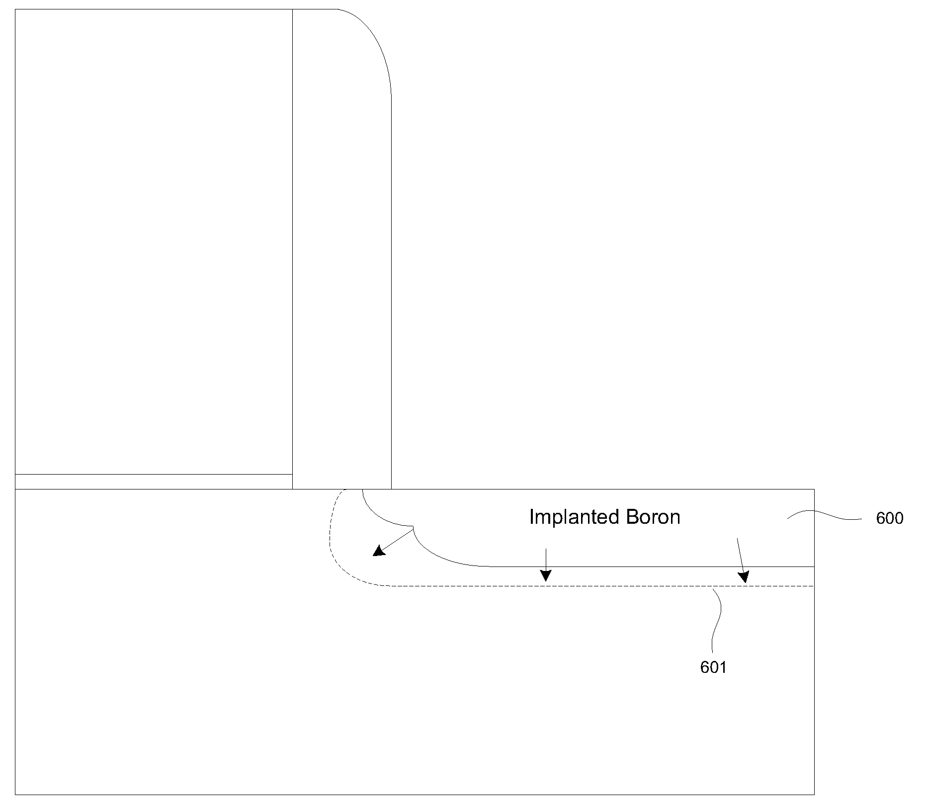
[0037]As stated above, silicon is typically a crystalline structure, where each silicon atom is tetrahedrally bonded to four neighboring silicon atoms. By bombarding this crystalline structure with atoms, such as silicon, germanium, or helium, the crystalline structure of the silicon workpiece can be altered. FIG. 3 is a substrate with an amorphous crystal structure. This crystal lattice 300 is implanted with ions 301 to cause this amorphous structure. This crystal lattice 300 which may be made up of, for example, silicon atoms, is amorphous, lacks a long-range order, and includes some atoms with dangling bonds. These ions 301 may be part of a helium PAI, for example. Since the crystal lattice 300 lacks a long-range order, the channels within the crystal lattice 300 do not exist. Thus, ions are unable to channel between the crystal lattice 300.

[0038]By bombarding ion to amorphize the substrate, channeling of implanted ions can be eliminated. However, while PAI eliminates the channel...


PUM


Abstract

A method of using helium to create ultra shallow junctions is disclosed. A pre-implantation amorphization using helium has significant advantages. For example, it has been shown that dopants will penetrate the substrate only to the amorphous-crystalline interface, and no further. Therefore, by properly determining the implant energy of helium, it is possible to exactly determine the junction depth. Increased doses of dopant simply reduce the substrate resistance with no effect on junction depth. Furthermore, the lateral straggle of helium is related to the implant energy and the dose rate of the helium PAI, therefore lateral diffusion can also be determined based on the implant energy and dose rate of the helium PAI. Thus, dopant may be precisely implanted beneath a sidewall spacer, or other obstruction.

Description

[0001]This application claims priority of U.S. Provisional Patent Application No. 61 / 088,809, filed on Aug. 14, 2008, the disclosure of which is hereby incorporated by reference.BACKGROUND OF THE INVENTION[0002]Ion implanters are commonly used in the production of semiconductor wafers. An ion source is used to create a beam of charged ions, which is then directed toward the wafer. As the ions strike the wafer, they impart a charge in the area of impact. This charge allows that particular region of the wafer to be properly “doped”. The configuration of doped regions defines their functionality, and through the use of conductive interconnects, these wafers can be transformed into complex circuits.[0003]FIG. 1 is a block diagram of a plasma doping system100, while FIG. 2 is a block diagram of a beam-line ion implanter 200. Those skilled in the art will recognize that the plasma doping system 100 and the beam-line ion implanter 200 are each only one of many examples of differing plasma ...

Claims


Application Information

Patent Timeline
IPC IPC(8): H01L21/266
CPCH01L21/2236H01L21/26506H01L29/7833H01L29/6659H01L21/26513H01L21/2658A61P31/04
Inventor HATEM, CHRISTOPHERGODET, LUDOVICKONTOS, ALEXANDER
Owner VARIAN SEMICON EQUIP ASSOC INC
Why Eureka
Try Eureka