Package for photoelectric wiring and lead frame

a technology of photoelectric wiring and lead frame, which is applied in the direction of instruments, optical elements, optics, etc., can solve the problems of loss of light signal, difficult to accurately dispose of mirror members on the board, and difficult to accurately set the tilt angle of the mirror, etc., to achieve convenient replacement of electric wiring, high precision, and easy form

Active Publication Date: 2010-02-25
SHINKO ELECTRIC IND CO LTD
View PDF4 Cites 15 Cited by
  • Summary
  • Abstract
  • Description
  • Claims
  • Application Information

AI Technical Summary

Benefits of technology

[0009]Exemplary embodiments of the present invention provide a package for a photoelectric wiring which can easily form, with high precision, a mirror for optically coupling an optical device to an optical waveguide and can readily replace an electric wiring with an optical wiring, and a lead frame which is used in the package.

Problems solved by technology

Referring to the method of disposing the mirror member on the board, however, it is hard to accurately dispose the mirror member on the board.
Moreover, there is a problem in that it is hard to accurately set a tilt angle of the mirror in the method of forming the mirror through the plating.
For this reason, there is a problem in that it is impossible to form the optical waveguide close to a mirror surface portion (the slant face portion), resulting in an increase in a spacing between the mirror surface portion and an end face of the optical waveguide to cause a loss of a light signal.

Method used


Image

  • Package for photoelectric wiring and lead frame
  • Package for photoelectric wiring and lead frame
  • Package for photoelectric wiring and lead frame

Examples


Embodiment Construction

[0038]Embodiments of a package for a photoelectric wiring according to the invention will be described below together with structures of a lead frame having a mirror section and a lead frame having an optical waveguide which are used in the package for a photoelectric wiring and methods of manufacturing them.

(Lead Frame having Mirror Section)

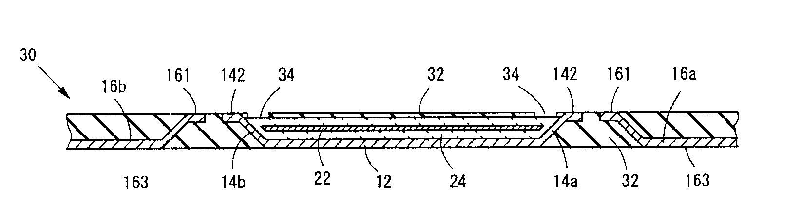
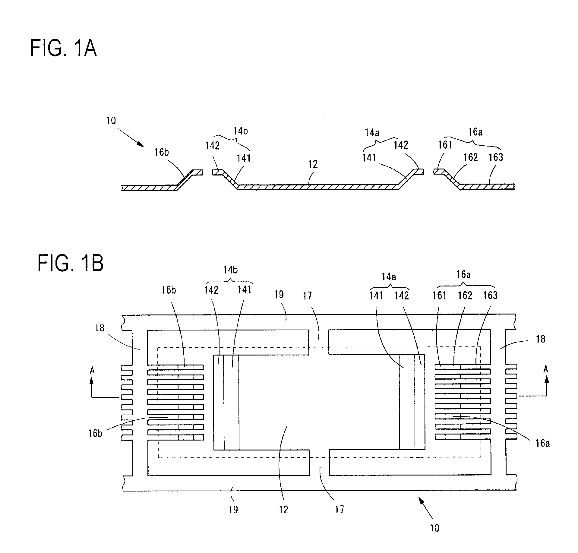
[0039]FIGS. 1A and 1B show a structure of a lead frame having a mirror section. FIG. 1A is a sectional view taken along an A-A line in FIG. 1B of a lead frame 10 having a mirror section and FIG. 1B is a plan view.

[0040]The lead frame 10 is formed by pressing a metallic band-shaped member in the same manner as a method of manufacturing a general lead frame. FIGS. 1A and 1B show a single unit portion of the lead frame 10 which is formed by pressing the metallic band-shaped member.

[0041]The lead frame 10 includes a support plate 12, mirror sections 14a and 14b, and lead portions 16a and 16b. The support plate 12 is formed to take a planar shape of ...


PUM


Abstract

A package for a photoelectric wiring in which a pair of light emitting and receiving devices are mounted as optical devices on a lead frame having an optical waveguide in which an optical waveguide having a plurality of core portions disposed in parallel and surrounded by a cladding is mounted on a support plate of a lead frame having a mirror section including the support plate for supporting the optical waveguide, mirror sections having a mirror surface portion formed by bending both edges of the support plate at an angle of 45 degrees with respect to a planar direction of the support plate in a side direction, and lead portions to be electrically connected to the optical devices, the support plate, the mirror sections and the lead sections being formed by pressing a metallic material, wherein the light emitting device and the light receiving device are mounted in alignment with an optical path of a light reflected by the mirror surface portion and transmitted through the core portions at one of sides and the other side which interpose the optical waveguide of the package for an optical waveguide wiring therebetween.

Description

[0001]This application claims priority to Japanese Patent Application No. 2008-215271, filed Aug. 25, 2008, in the Japanese Patent Office. The Japanese Patent Application No. 2008-215271 is incorporated by reference in its entirety.TECHNICAL FIELD[0002]The present disclosure relates to a package for a photoelectric wiring including an optical waveguide for transmitting a light signal and an optical device for converting a light signal and an electric signal, and a lead frame which is used in the package.RELATED ART[0003]With an increase in a speed of a semiconductor device such as a microprocessor, there has been investigated a method of replacing an electric wiring to be used for transmitting a signal with an optical wiring and transmitting the signal by utilizing the optical wiring. In order to replace the electric wiring with the optical wiring, it is preferable to replace the electric wiring through an optical waveguide, to dispose optical devices (a light emitting device and a ...

Claims


Application Information

Patent Timeline
Patent Type & Authority Applications(United States)
IPC IPC(8): H01L27/15H01L23/495
CPCG02B6/4214H01L2224/16245G02B6/43
Inventor YAMAMOTO, TAKANORI
Owner SHINKO ELECTRIC IND CO LTD
Why Eureka
Try Eureka