Layout Method for a Chip

a chip and layout technology, applied in the field of integrated circuit design, can solve the problems of insufficient routing resources, inability to meet timing criterion, and inducing considerable costs, and achieve the effect of reducing the possibility of hotspots

Inactive Publication Date: 2010-02-25
ALICORP
View PDF3 Cites 10 Cited by
  • Summary
  • Abstract
  • Description
  • Claims
  • Application Information

AI Technical Summary

Benefits of technology

[0010]An exemplary embodiment of a layout method is provided, adaptable to place cells on a chip. Firstly, a chip area is assigned for a floor plan. A global reservation deployment process is then performed to define a plurality of room units to be uniformly distributed on the chip area. Cells are placed on the chip based on the floor plan. The chip area is categorized into at least a high frequency region and a low frequency region according to operation frequencies of the cells placed thereon. A frequency based reservation deployment process is then performed to move one or more room units distributed in the low frequency region toward the high frequency region. A local cell replacement process is performed for the placed cells based on the distribution of the room units to decrease possibility of hotspots. A routing and timing analysis is performed to determine whether hotspots are induced from the cells placement. If hotspots are induced, room units around the hotspots are redistributed, and then the steps of local cell replacement, routing and timing analysis are repeated.

Problems solved by technology

One is a routing hotspot, wherein routing resource is not enough to accomplish wire connection between components.
Another is a timing hotspot, wherein operation frequencies in the region cannot meet the timing criterion.
In practice, chip area is a limited resource, and mitigating the hotspots by enlarging chip area could induce considerable costs.
Thus, the conventional approach is cost ineffective and produces less competitive products.

Method used


Image

  • Layout Method for a Chip
  • Layout Method for a Chip
  • Layout Method for a Chip

Examples


Embodiment Construction

[0032]The following description is of the best-contemplated mode of carrying out the invention. This description is made for the purpose of illustrating the general principles of the invention and should not be taken in a limiting sense. The scope of the invention is best determined by reference to the appended claims.

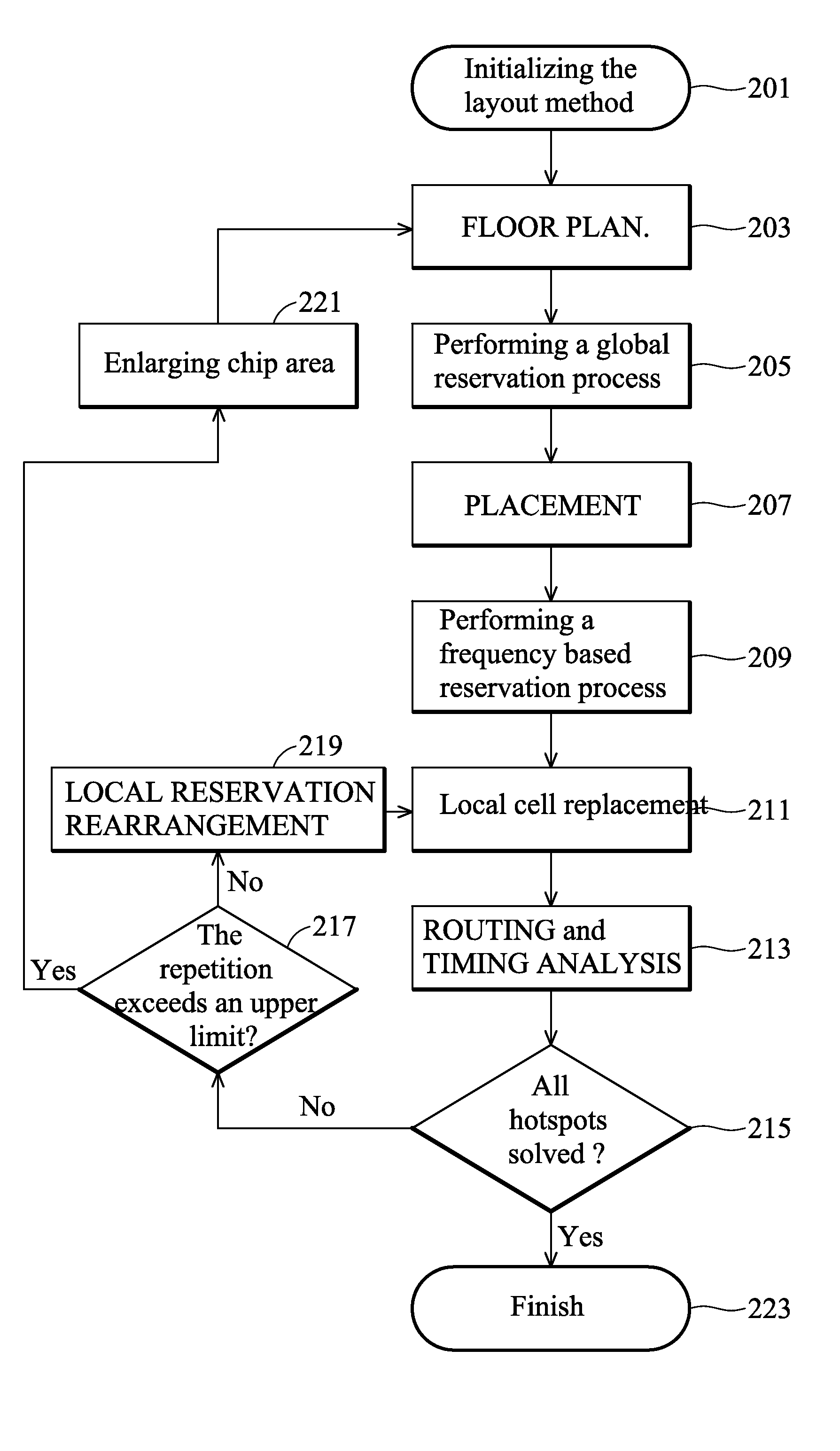
[0033]FIG. 2 is a flowchart of a layout method according to an embodiment of the invention. In the invention, an approach for reserving areas is proposed. The reservation deployment is achieved by packaging reserved space into standard cell styles, hereby referred to as room units. Operation frequencies of cells are taken as a basis for distributing the room units, thereby increasing efficiency of a successive routing process, as well as area utilization rate. In step 201, the layout method is initialized. In step 203, a floor plan is performed on the substrate of the SOC, whereby design rules and fundamental structure are defined. The floor plan is a known prior art p...


PUM


Abstract

A layout method is provided, adaptable to place cell on a chip. Firstly, a chip area is assigned for a floor plan. A global reservation deployment process is then performed to define a plurality of room units to be uniformly distributed on the chip area. Cells are placed on the chip based on the floor plan. The chip area is categorized into at least a high frequency region and a low frequency region according to operation frequencies of the placed cells thereon. A frequency based reservation deployment process is then performed to move one or more room units distributed in the low frequency region toward the high frequency region. A local cell replacement process, a routing and timing analysis are performed. If hotspots are induced, room units around the hotspots are redistributed, and then the steps of local cell replacement, routing and timing analysis are repeated.

Description

CROSS REFERENCE TO RELATED APPLICATIONS[0001]This Application claims priority of China Patent Application No. 200810212621.0, filed on Aug. 25, 2008 the entirety of which is incorporated by reference herein.BACKGROUND OF THE INVENTION[0002]1. Field of the Invention[0003]The invention relates to integrated circuit design, and in particular, to a layout method for standard cell placement on a system on chip.[0004]2. Description of the Related Art[0005]A system on chip (SOC) comprises thousands or millions of standard cells (also referred to as “cells”), such as logic units, AND gates, OR gates, and registers. Hence, an Electronic Design Automation (EDA) tool is required to help design an SOC. Conventionally, a floor plan (FLOOR PLAN) is performed to deposit analog modules, memory modules and IO pads on particular locations on the SOC. Other cells are then placed (PLACEMENT) on appropriate locations, and thereafter, a routing process (ROUTING) is performed.[0006]FIG. 1a shows a convent...

Claims


Application Information

Patent Timeline
Patent Type & Authority Applications(United States)
IPC IPC(8): G06F17/50
CPCG06F17/5081G06F17/5031G06F30/398G06F30/3312
Inventor CHANG, CHUNG-CHIAOCHEN, JIAN-LIANG
Owner ALICORP
Why Eureka
Try Eureka