

Thin-film transistor and method of manufacturing same
a thin film transistor and transistor technology, applied in the field of thin film transistors, can solve the problems of increasing power consumption, no favorable tft characteristics, etc., and achieve the effect of reducing power consumption
- Summary
- Abstract
- Description
- Claims
- Application Information
AI Technical Summary
Benefits of technology
Problems solved by technology
Method used
Image

Examples
exemplary embodiment 1
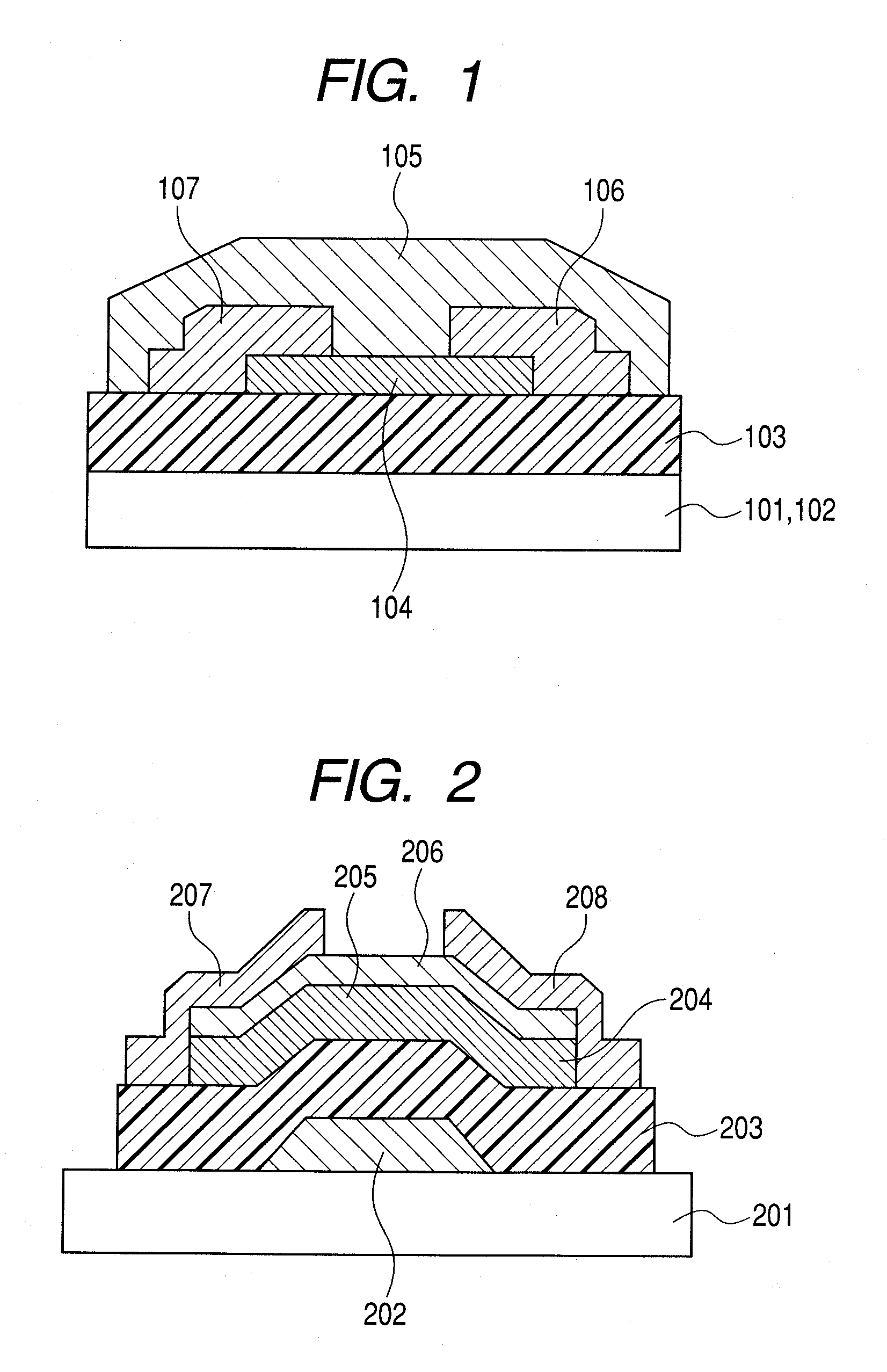
[0052]In the present exemplary embodiment, a bottom-gate (inversely staggered) TFT illustrated in FIG. 1 was fabricated. The TFT in FIG. 1 uses low-resistance n-type crystalline silicon for a substrate 101 also serving as a gate electrode 102, and a thermal silicon oxide for a gate insulating film 103. The TFT further includes an oxide semiconductor 104, a protective layer 105, a source electrode 106 and a drain electrode 107.
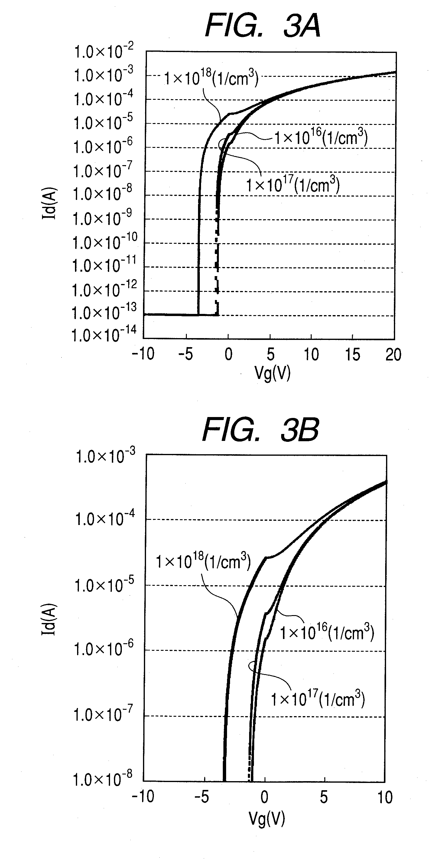
[0053]First, a 20 nm thick In—Ga—Zn—O oxide semiconductor was deposited by an RF sputtering method on the low-resistance n-type crystalline silicon substrate as the oxide semiconductor layer 104, using a polycrystalline sintered object having an InGaO3 (ZnO) composition as a target. In the present exemplary embodiment, the RF power applied at that time was 200 W. The atmosphere applied at the time of film-forming was at a full pressure of 0.5 Pa, and the gas flow rate ratio at that time was Ar:O2=95:5. The film-forming rate was 8 nm / min. In addition, the substr...
exemplary embodiment 2
[0067]In the present exemplary embodiment, the bottom-gate TFT illustrated in FIG. 4 was fabricated.
[0068]As a substrate 401, a Corning 1737 glass substrate was used. First, a 5 nm thick Ti film, a 50 nm thick Au film, and another 5 nm thick Ti film were deposited in this order on the substrate 401 by an electron beam deposition method. The deposited films were formed into a gate electrode 402 by photolithography and lift-off methods. In addition, a 200 nm thick SiO2 film was formed on top of the electrode by an RF sputtering method to form a gate insulating layer 403. Subsequently, a 20 nm thick In—Ga—Zn—O oxide semiconductor was deposited as a channel layer 404 by an RF sputtering method using a polycrystalline sintered object having an InGaO3 (ZnO) composition as a target.
[0069]In the present exemplary embodiment, the RF power applied was 200 W. The atmosphere applied at the time of film-forming was at a full pressure of 0.5 Pa, and the gas flow rate ratio at that time was Ar:O2=...
exemplary embodiment 3
[0074]In the present exemplary embodiment, a display unit using the TFT illustrated in FIG. 4 will be described.
[0075]First, a method of manufacturing the TFT will be described using FIG. 4.
[0076]As a substrate 401, a Corning 1737 glass substrate was used. A 150 nm thick ITO film was formed on the substrate 401 by a sputtering method. Next, a gate electrode 402 was formed using photolithography and etching methods. In addition, a 200 nm thick SiO2 film was formed on top of the gate electrode by an RF sputtering method, to form a gate insulating layer 403. Subsequently, a 20 nm thick In—Ga—Zn—O oxide semiconductor was deposited as a channel layer 404 by an RF sputtering method using a polycrystalline sintered object having an InGaO3 (ZnO) composition as a target. In the present exemplary embodiment, the RF power applied at that time was 200 W. The atmosphere applied at the time of film-forming was at a full pressure of 0.5 Pa, and the gas flow rate ratio at that time was Ar:O2=95:5. ...
PUM
 Abstract
Description
Claims
Application Information