
High density flash memory device and fabricating method thereof

Active Publication Date: 2010-03-04
SEOUL NAT UNIV R&DB FOUND
View PDF5 Cites 28 Cited by
  • Summary
  • Abstract
  • Description
  • Claims
  • Application Information

AI Technical Summary

Benefits of technology

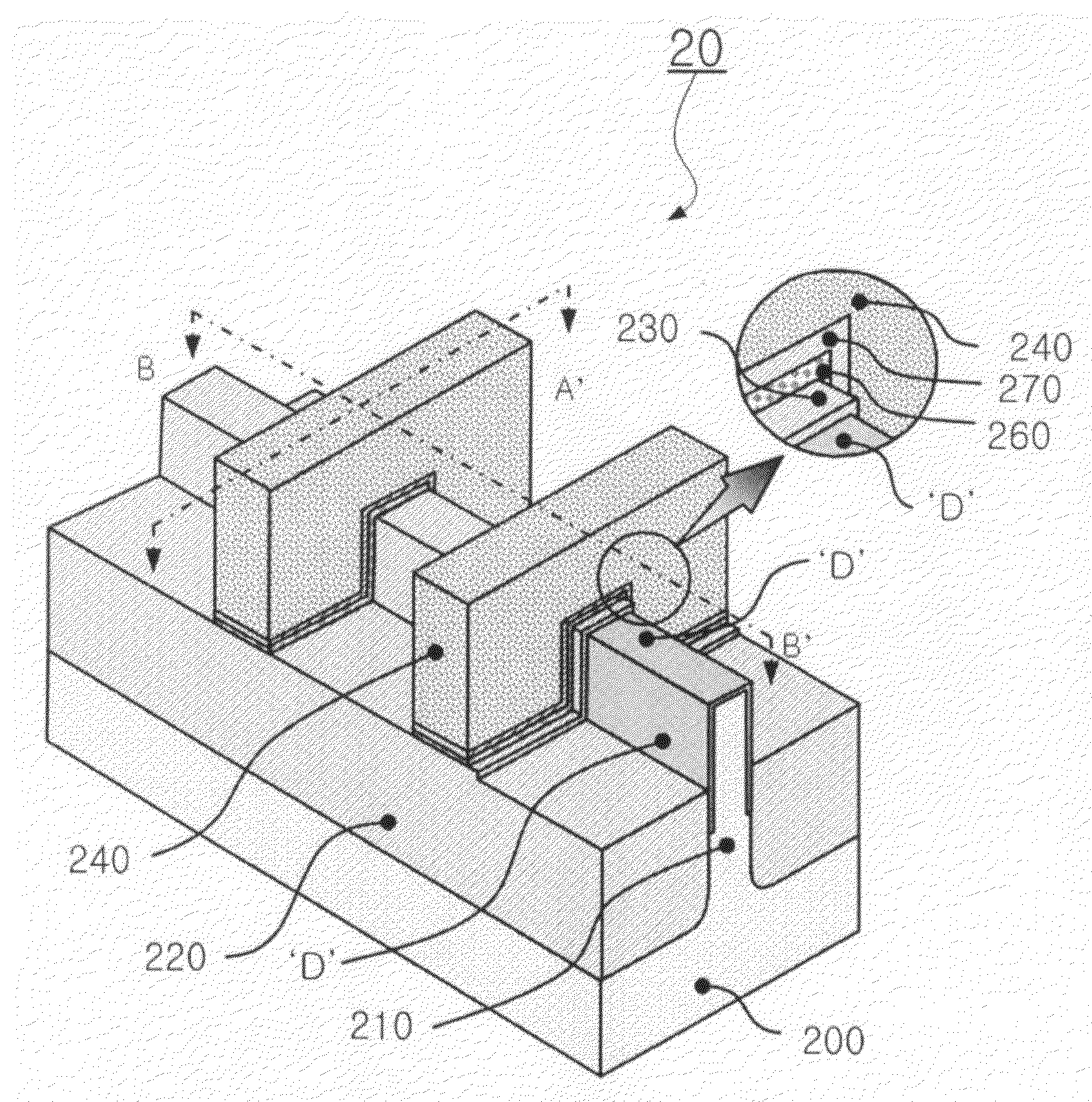
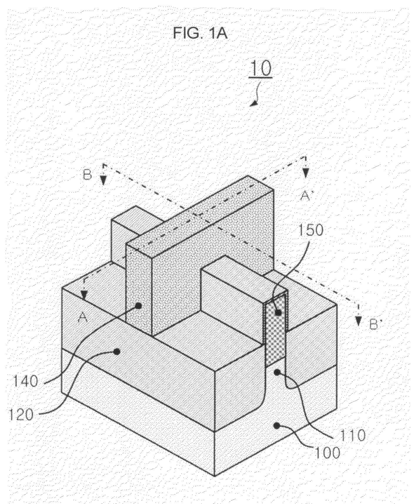
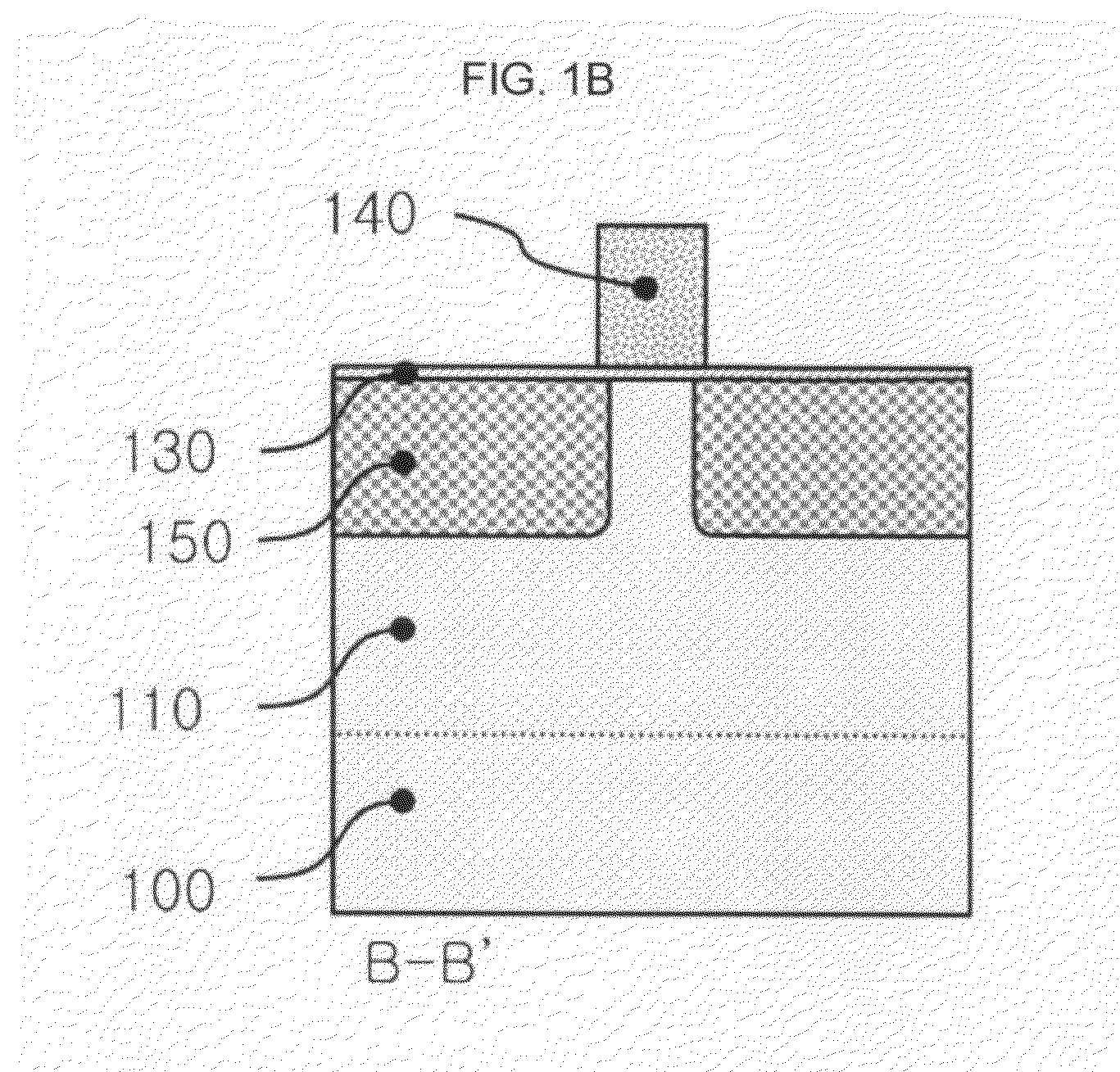
[0019]According to the present invention, a NAND flash memory cell constituting a cell string of a NAND flash memory is constructed as a cell device having a double / triple-gate structure where there are no source / drain regions or the source / drain regions are not overlapped with a control electrode, so that a short channel effect can be effectively suppressed even in a gate length of equal to or less than 40 nm in comparison with an existing double / triple-gate structure. Accordingly, miniaturization characteristics can be further improved.
[0020]In addition, in comparison with an SONOS-type NAND flash cell device having an existing planar channel structure, in a cell device according to the present invention, it is possible to obtain a high degree of integration due to the double / triple-gate structure. In addition, in a memory device having an existing planar channel where an inversion layer cannot be easily formed, in a memory device having a structure according to the present invention, there are no source / drain regions or the source / drain regions that are not overlapped with a control electrode are formed by using a wall-shaped body, so that the inversion layer can be easily formed by a fringing field generated from a side surface of the control electrode.
[0021]In addition, according to the present invention, source / drain regions are not formed in a cell device of a NAND string, and although the source / drain regions are formed in the cell device, the source / drain regions are not overlapped with a control electrode, so that gate induced drain leakage (GIDL) is relatively small. Accordingly, it is possible to further reduce an off-state current. In particular, according to the present invention, in a case where the source / drain regions are not formed in the cell device, a junction leakage current does not occur between the source / drain regions and a substrate. In addition, according to the present invention, although the source / drain regions that are not overlapped with the control electrode are formed in the cell device, since widths of the source / drain regions are small, so that the junction leakage current can be reduced.

Problems solved by technology

Accordingly, a short channel effect becomes a big problem in the NAND flash device having a planar channel structure including an existing conductive floating gate, and thus, there is a limitation to reduce the gate length.
Since the short channel effect due to device miniaturization increases dispersion of a threshold voltage in the multi-level cell, there is a limitation or impossibility to use the multi-level cell.
However, although the improved storage electrode is used, in a case where the gate length is equal to or less than 40 nm, it is difficult or impossible to miniaturize a memory cell due to a short channel effect.
As a result, there is a limitation to miniaturize a cell device having a planar channel structure.
Accordingly, there is a problem in that characteristics of the device deteriorate, and non-uniformity of the device increase.

Method used


Image

  • High density flash memory device and fabricating method thereof
  • High density flash memory device and fabricating method thereof
  • High density flash memory device and fabricating method thereof

Examples


first embodiment

[0051]Now, a NAND flash memory device according to a first embodiment of the present invention will be described in detail with reference to FIG. 6. The memory device according to the first embodiment of the present invention is characterized in that source / drain regions are separated by a predetermined distance from control electrodes so as for the source / drain regions not to be overlapped with the control electrode. In FIG. 6, (a) is a perspective view illustrating a portion of a cell string of the NAND flash memory, that is, the memory device according to the first embodiment of the present invention, in which two devices are provided to the cell string, that is, in which two word lines are provided. In FIG. 6, (b) is a plan view of (a) of FIG. 6, (c) is a cross-sectional view taken along line B-B′, and (c) is a cross-sectional view taken along line A-A′. Referring to FIG. 6, the flash memory device 60 according to the first embodiment of the present invention includes a bulk sil...


PUM


Abstract

The present invention provides a flash memory device having a high degree of integration and high performance. The flash memory device has a double / triple gate structure where a channel is formed in a wall-shaped body. The flash memory device has no source / drain regions. In addition, although the flash memory device has the source / drain regions, the source / drain region are formed not to be overlapped with a control electrode. Accordingly, an inversion layer is induced by a fringing field generated from the control electrode, so that cell devices can be electrically connected to each other. The flash memory device includes a charge storage node for storing charges formed under the control electrode, so that miniaturization characteristics of cell device can be improved. According to the present invention, there is proposed a new device capable of improving the miniaturization characteristics of a MOS-based flash memory device and increasing memory capacity.

Description

TECHNICAL FIELD[0001]The present invention relates to a flash memory device and a fabricating method thereof, and more particularly, a flash memory device having a new structure capable of improving miniaturization characteristics and performance of a MOSFET-based flash memory device and increasing memory capacity thereof and a fabricating method thereof.BACKGROUND ART[0002]Recently, since demands on a flash memory greatly increase in consumer electronics and mobile electric devices, a market of the flash memory is expected to exceed a market of an existing DRAM in 2007. Therefore, a memory device with a high integration degree and a short write / erase time has been required. The integration degree of a NAND flash memory has been required to increase, as IT techniques are developed. The integration degree of the NAND flash memory greatly depends on an integration degree of cell devices constituting the memory. Recently, a length of each cell device constituting the NAND flash memory ...

Claims


Application Information

Patent Timeline
IPC IPC(8): H01L29/792
CPCH01L27/115H01L27/11519H01L29/42332H01L29/42348H01L29/785H01L29/7923H01L29/7854H01L29/7881H01L29/7887H01L29/792H01L29/7851H10B41/10H10B69/00H10B43/10H01L29/40117
Inventor LEE, JONG-HO
Owner SEOUL NAT UNIV R&DB FOUND
Learn More