Method of manufacturing semiconductor device

a manufacturing method and semiconductor technology, applied in the direction of semiconductor devices, electrical appliances, transistors, etc., can solve the problems of poor refresh property, difficult to perform normal read and write operations, and many difficulties, and achieve the effect of increasing the length of the effective channel

Active Publication Date: 2010-03-04
SK HYNIX INC
View PDF4 Cites 4 Cited by
  • Summary
  • Abstract
  • Description
  • Claims
  • Application Information

AI Technical Summary

Benefits of technology

[0008]Various embodiments of the invention are directed to providing a method of manufacturing a semiconductor memory device and a semiconductor memory device manufactured using the same, wherein, in a process of forming the source / drain regions of a floating body transistor, the source / drain regions are etched through an etch process using a mask, so that neighboring floating body transistors can be electrically isolated from each other and the length of an effective channel can be increased.

Problems solved by technology

In order to overcome this problem and increase the electrostatic capacitance of the capacitor, an effort is being made to develop a semiconductor device constituting an insulating layer within the capacitor, but have encountered many difficulties.
The decrease of the design rule makes it difficult to perform normal read and write operations because the value of junction resistance at a storage node SN within the unit cell and the turn-on resistance value of the transistor rise, resulting in a poor refresh property.

Method used


Image

  • Method of manufacturing semiconductor device
  • Method of manufacturing semiconductor device
  • Method of manufacturing semiconductor device

Examples


Embodiment Construction

[0028]Hereinafter, an embodiment of the present disclosure will be described in detail with reference to accompanying drawings.

[0029]A semiconductor memory device using a floating body effect is first described.

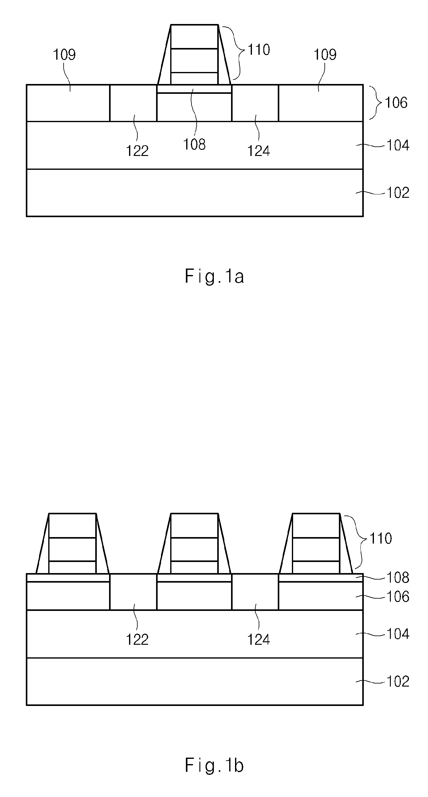
[0030]FIGS. 1a and 1b are cross-sectional views of a floating body transistor within a semiconductor device formed in a SOI substrate.

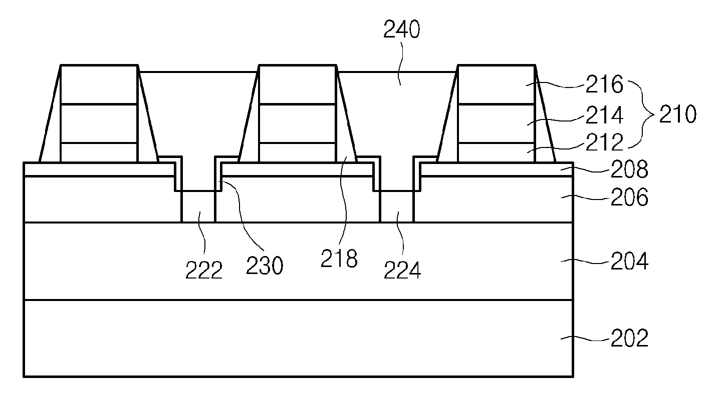
[0031]Referring to FIG. 1a, a floating transistor is formed in an SOI substrate, including a lower semiconductor substrate 102, a buried insulating layer 104, and an upper silicon layer 106. The upper silicon layer 106 remains in an active region, and the active regions are isolated from each other by an isolation layer 109. A gate oxide layer 108 is deposited on the active region, and a gate pattern 110 is formed on the gate oxide layer 108. A source region 122 and a drain region 124 are placed on both sides of the gate pattern 110.

[0032]Referring to FIG. 1b, a plurality of floating body transistors are formed in the respective upper silicon l...


PUM


Abstract

The present invention relates to a method of manufacturing a semiconductor memory device and a semiconductor memory device manufactured using the same. A method of manufacturing a semiconductor device comprises defining source/drain regions in semiconductor substrate through an etch process using a mask, and forming a gate and source/drain by depositing a conductive material over the defined regions and the semiconductor substrate and patterning the conductive material.

Description

CROSS-REFERENCE TO RELATED APPLICATION[0001]The present application claims priority to Korean patent application number 10-2008-0085854, filed on Sep. 1, 2008, which is incorporated by reference in its entirety.BACKGROUND OF THE INVENTION[0002]The present invention relates to a method of manufacturing a semiconductor device and, more particularly, to a technology related to a process of forming transistors for a high-integrated semiconductor memory device using a Silicon-On-Insulator (SOI) substrate.[0003]In a system including a plurality of electronic components, a semiconductor memory device is used to store data. When a data processing device (e.g., a Central Processing Unit (CPU)) requests data, a semiconductor memory device outputs stored data corresponding to an address received from a data request apparatus.[0004]With an increase in the data storage capacity of a semiconductor memory device, the size of a unit cell has gradually decreased and the size of an element for a read...

Claims


Application Information

Patent Timeline
Patent Type & Authority Applications(United States)
IPC IPC(8): H01L29/786H01L21/336
CPCH01L21/84H01L27/108H01L29/7841H01L27/1203H01L27/10802H10B12/20H10B12/00
Inventor LEE, JAE YEON
Owner SK HYNIX INC
Why Eureka
Try Eureka