Chip scale package structure and fabrication method thereof

a technology of chip scale and package structure, applied in the direction of electrical equipment, semiconductor devices, semiconductor/solid-state device details, etc., can solve the problems of increasing heat dissipation issues, laborious and time-consuming packaging process, etc., to improve heat dissipation, improve the reliability of the resultant package structure, and simple process steps

Inactive Publication Date: 2010-03-04
ADVANCED SEMICON ENG INC
View PDF13 Cites 10 Cited by
  • Summary
  • Abstract
  • Description
  • Claims
  • Application Information

AI Technical Summary

Benefits of technology

[0017]In view of the above, as the matrix heat sink is used, better heat dissipation is achieved along with straightforward a

Problems solved by technology

However, the packaging process is laborious and time-consuming as each heat spreader is placed over the c

Method used


Image

  • Chip scale package structure and fabrication method thereof
  • Chip scale package structure and fabrication method thereof
  • Chip scale package structure and fabrication method thereof

Examples


Embodiment Construction

[0024]Reference will now be made in detail to the present preferred embodiments of the invention, examples of which are illustrated in the accompanying drawings.

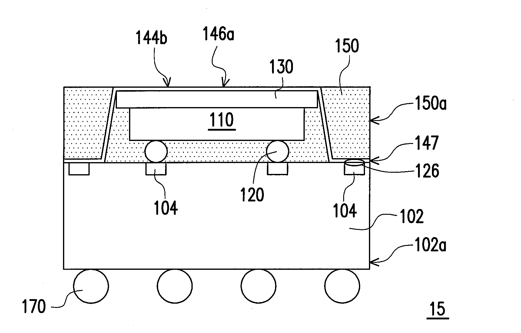
[0025]The following preferred embodiments focus on chip scale package (CSP) technology as examples, but the scope of the present invention will not be limited by the descriptions or embodiments herein. In addition to CSP technology, wafer-level chip scale package (WLCSP) technology, ball grid array (BGA) technology or area-array flip chip technology may be applicable for fabricating the package structure encompassed with the scope of this invention. Moreover, a variety of techniques of the CSP technology, such as, the single chip package, the stack chip package and the planar multi-chip package (MCM) may also be applicable if considered appropriate.

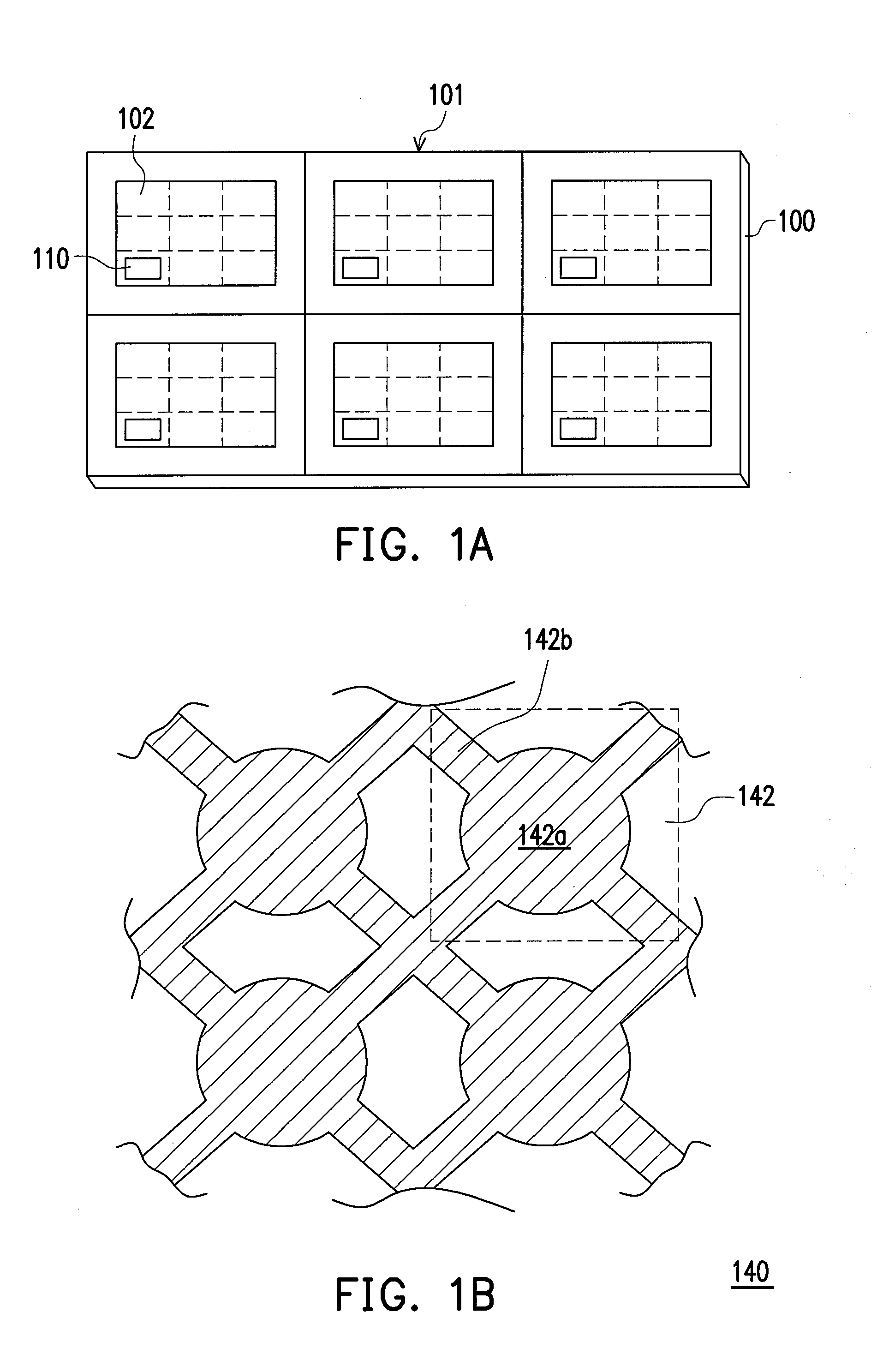
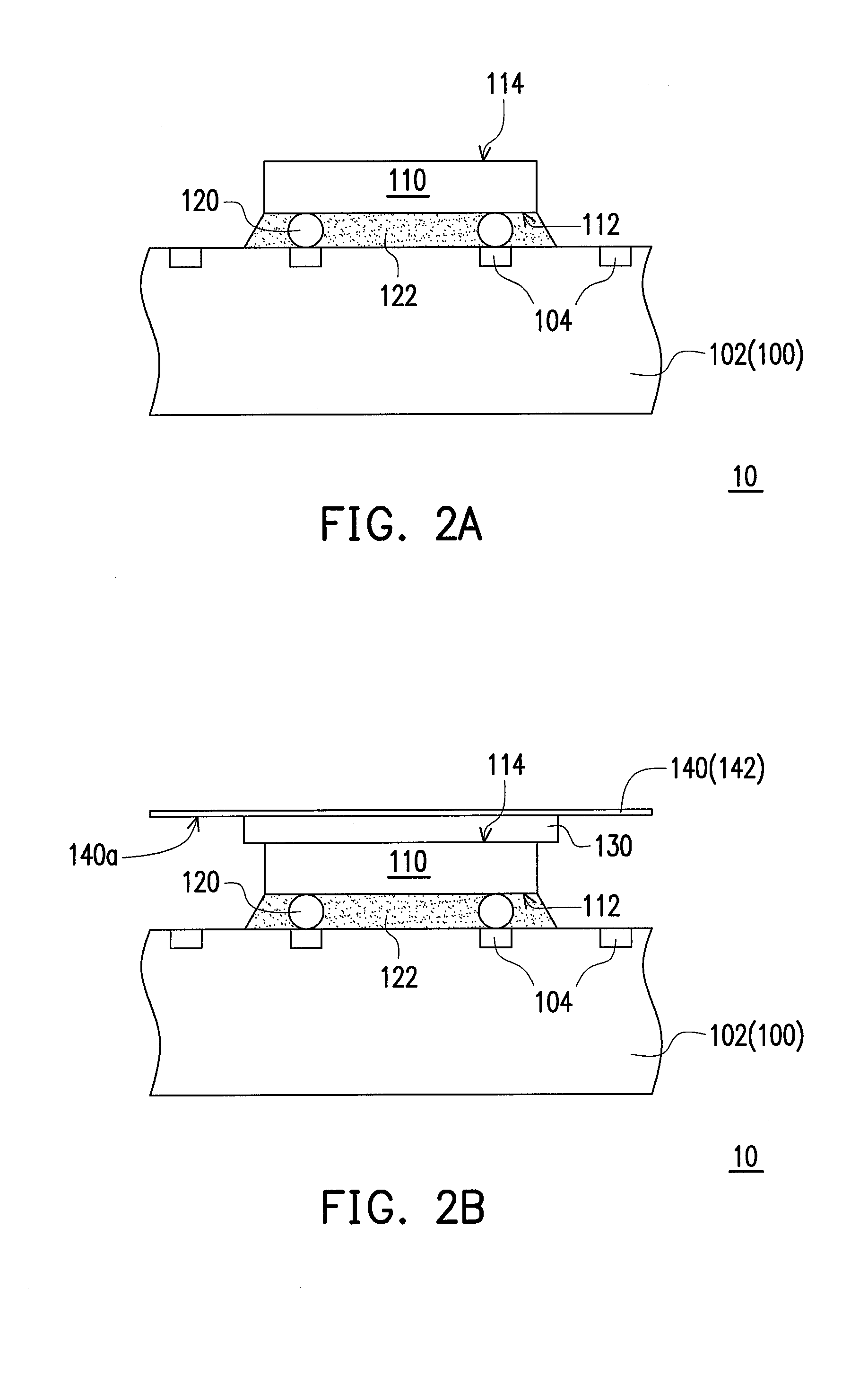
[0026]FIG. 1A is a top view of a package substrate according to one embodiment of the invention. FIGS. 2A-2E are schematic cross-sectional views of a chip scale packaging process ...


PUM


Abstract

A chip scale package (CSP) structure and the packaging process thereof are described. By using a matrix of interlinked heat sink units compatible with the block substrate, the packaging process can be simplified and a plurality of packages units or chip scale packages with enhanced thermal performance can be obtained after singulation.

Description

BACKGROUND OF THE INVENTION[0001]1. Field of Invention[0002]The present invention relates to a chip package structure and the fabrication method thereof. More particularly, the present invention relates to a chip scale package (CSP) structure and the fabrication method thereof.[0003]2. Description of Related Art[0004]Along with the size shrinkage of chips, increased operation speeds of electronic devices and high-level package density, the amount of heat generated within a semiconductor package has been increased considerably. In order to improve the heat dissipation ability of the package structure, it is common to employ a heat dissipation plate or a heat sink for assisting heat dissipation of the chip.[0005]Taking the conventional ball grid array (BGA) package structure as an example, a heat spreader is placed above the chip and adhered to the substrate by an adhesive material. However, the packaging process is laborious and time-consuming as each heat spreader is placed over the...

Claims


Application Information

Patent Timeline
IPC IPC(8): H01L23/36H01L21/56
CPCH01L21/563H01L23/3114H01L2924/01006H01L24/48H01L2924/3025H01L2924/16152H01L2924/15311H01L2924/01082H01L2924/01075H01L2924/01033H01L2924/01029H01L2924/01013H01L2924/01005H01L2224/97H01L2224/73253H01L2224/73204H01L2224/73203H01L23/3128H01L23/4334H01L23/49816H01L24/97H01L2224/16225H01L2224/48091H01L2224/48227H01L2924/00014H01L2224/81H01L2224/73265H01L2924/181H01L2224/04042H01L2224/8592H01L2224/32245H01L2924/00011H01L2224/0401H01L2924/00012H01L2224/45099H01L2224/45015H01L2924/207
Inventor APPELT, BERND KARLFACTOR, BRADFORD J.
Owner ADVANCED SEMICON ENG INC
Why Eureka
Try Eureka