Integrated optical latch

a latch and optical technology, applied in the field of optical communication, can solve the problems of reducing the speed at which the gate can switch, reducing the efficiency of the latch, and reducing the efficiency of the latch, and achieve the effect of high index contrast (hic) and high index contrast (hic)

Active Publication Date: 2010-03-04
BAE SYST INFORMATION & ELECTRONICS SYST INTERGRATION INC
View PDF74 Cites 22 Cited by
  • Summary
  • Abstract
  • Description
  • Claims
  • Application Information

AI Technical Summary

Benefits of technology

[0005]One embodiment of the present invention provides an integrated optical circuit device. The device includes a first integrated waveguide loop for guiding optical signals, a nonlinear phase shifting element for phase shifting signals in the first waveguide loop, a tunable coupler for providing an input pulse in both clockwise and counter-clockwise direction of the first waveguide loop, and an input coupler for providing a control pulse in at least one direction of the first waveguide loop. The first waveguide loop can be, for example, a high index contrast (HIC) silicon waveguide. The nonlinear phase shifting element may include, for example, n individually tunable resonant elements. In one such case, the nonlinear phase shifting element includes a salicide heater structure for providing heat to the n individually tunable resonant elements. The nonlinear phase shifting element may include one or more tunable couplers configured with salicide heating elements for optically coupling resonant elements to the first waveguide loop. Such heaters can be used to change the effective phase delay and coupling coefficient associated with such optical elements. In one specific embodiment, the first waveguide loop is configured with an inner ring and an outer ring optically coupled to the inner ring, and the nonlinear phase shifting element is in the inner ring. The device may includes a second integrated waveguide loop for guiding optical signals, a nonlinear phase shifting element for phase shifting signals in the second waveguide loop, a tunable coupler for providing an input pulse in both clockwise and counter-clockwise direction of the second waveguide loop, and an input coupler for providing a control pulse in at least one direction of the second waveguide loop. The second waveguide can be, for example, a high index contrast (HIC) silicon waveguide. The nonlinear phase shifting element for phase shifting signals in the second waveguide loop may include, for example, n individually tunable resonant elements. In one such case, the nonlinear phase shifting element for phase shifting signals in the second waveguide loop includes a salicide heater structure for providing heat to the n individually tunable resonant elements. The nonlinear phase shifting element for phase shifting signals in the second waveguide loop may include one or more tunable couplers configured with salicide heating elements for optically coupling resonant elements to the second waveguide loop. In another specific embodiment, the second waveguide loop is configured with an inner ring and an outer ring optically coupled to the inner ring, and nonlinear phase shifting element for phase shifting signals in the second waveguide loop is in the inner ring.

Problems solved by technology

In some such applications, however, the speed at which the gates can switch is limited, by both the gates themselves as well as the clocking signals that enable the switching.
Although optical circuits can be used to improve speed, there are oftentimes still instances where optical circuitry interfaces with electronic circuitry, giving rise to switching delays.
This conversion adds complexity and cost, in addition to delays associated with the conversion process itself as well as with switching delays.

Method used


Image

  • Integrated optical latch
  • Integrated optical latch
  • Integrated optical latch

Examples


Embodiment Construction

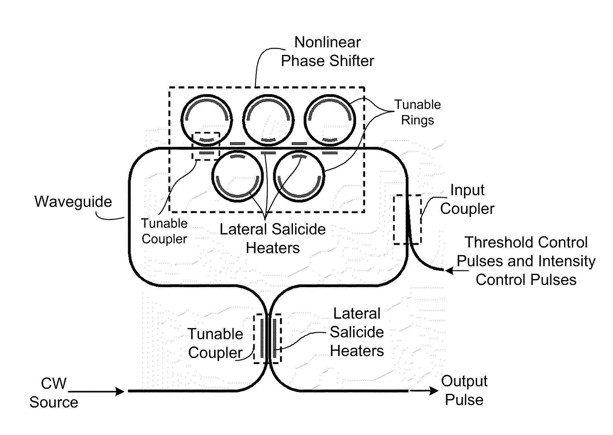
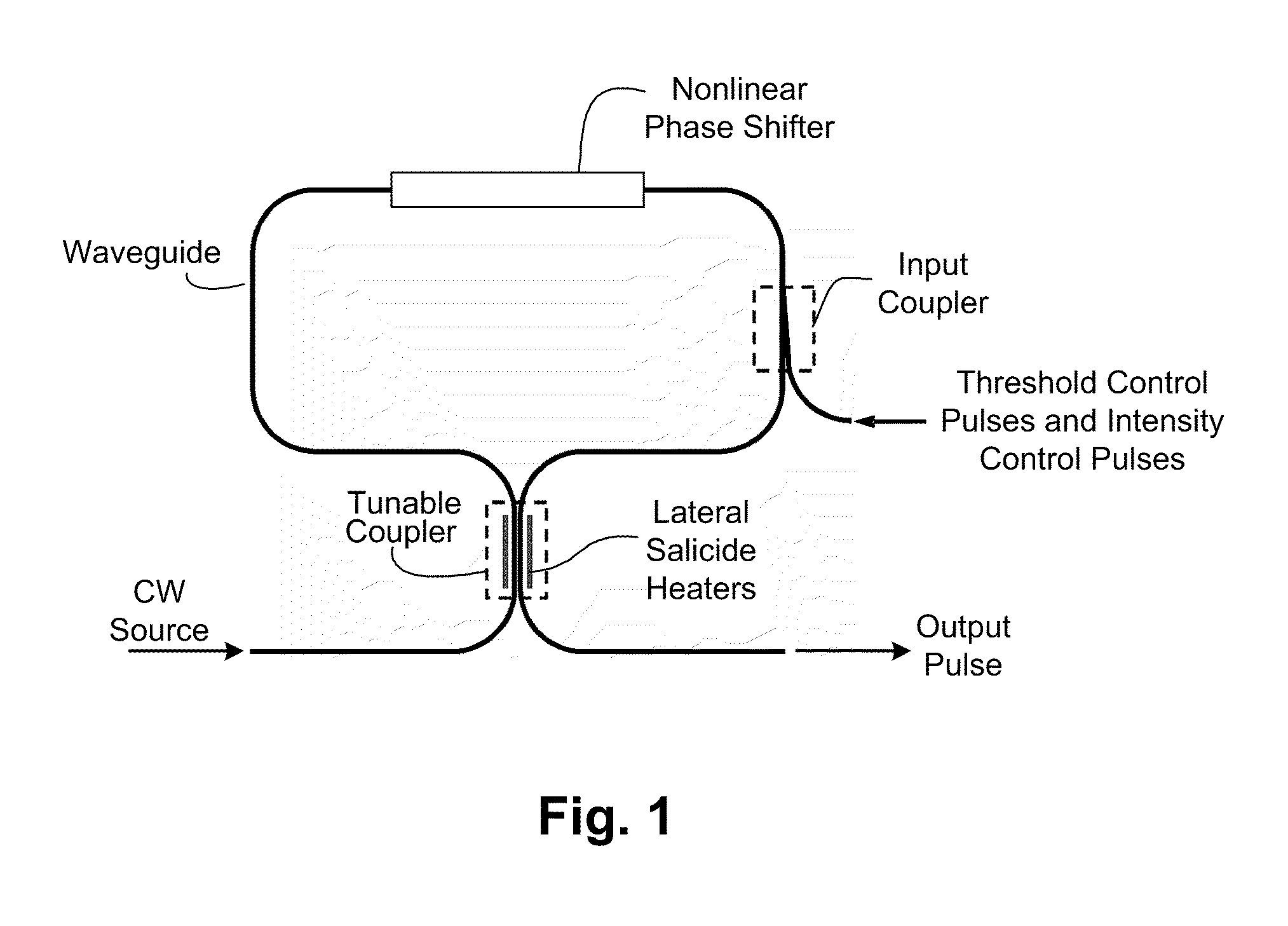
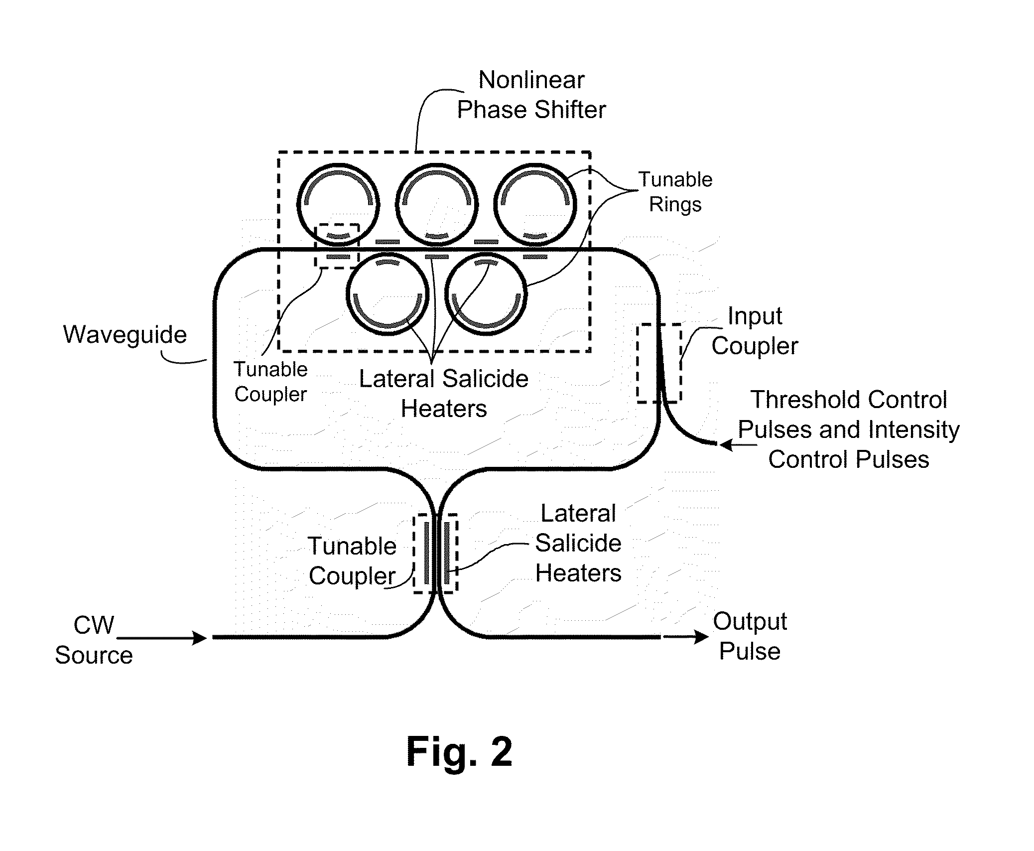
[0011]Techniques are disclosed for optical switching and data control without the interaction of electronic switching speeds.

[0012]In one example embodiment, a common cavity optical latch is provided that takes advantage of the fact that dense integration of low loss waveguides in silicon can be achieved in a way that allows precise control of phase. This control of the optical phase allows optical modal switching to be employed between two common optical cavities, using incident optical signals and the way in which the cavities manipulate the phase within them to lock in one or the other configuration, thereby forming an optical latch.

[0013]The optical latch is implemented in an integrated fashion, such as in a CMOS environment on a silicon substrate. Such an optical latch can be used, for example, in almost any application where a data bus is required. Numerous applications will be apparent, such as in optical computers and data transmission systems, or other such systems where it...


PUM

PropertyMeasurementUnit
voltageaaaaaaaaaa
thicknessaaaaaaaaaa
nonlinear phaseaaaaaaaaaa

Abstract

Techniques are disclosed for optical switching and data control, without the interaction of electronic switching speeds. In one example embodiment, a common cavity optical latch is provided that that can hold an optical state for an extended period of time, and the operation of which is controlled optically. Optical phase control allows optical modal switching to be employed between two common optical cavities, using incident optical signals and the way in which the cavities manipulate the phase within them to lock in one or the other configuration, thereby forming an optical latch. The optical latch is implemented in an integrated fashion, such as in a CMOS environment.

Description

RELATED APPLICATIONS[0001]This application is related to U.S. application Ser. No. ______ (Attorney Docket 20070094), filed Aug. 29, 2008, and titled “Salicide Structures for Heat-Influenced Semiconductor Applications” which is herein incorporated by reference in its entirety. This application is also related to U.S. application Ser. No. ______ (Attorney Docket 20070095), filed Aug. 29, 2008, and titled “Two-Step Hardmask Fabrication Methodology for Silicon Waveguides” which is herein incorporated by reference in its entirety.FIELD OF THE INVENTION[0002]The invention relates to optical communications, and more particularly, to an optical latch.BACKGROUND OF THE INVENTION[0003]Digital electronics such as logic gates are commonly used in implementing circuits of all kinds. In some such applications, however, the speed at which the gates can switch is limited, by both the gates themselves as well as the clocking signals that enable the switching. Although optical circuits can be used t...

Claims


Application Information

Patent Timeline
Patent Type & Authority Applications(United States)
IPC IPC(8): G02F3/00G02B6/12
CPCG02F1/0147G02F1/225G02F2203/15G02F2001/211G02F1/3519G02F1/211
Inventor CAROTHERS, DANIEL N.
Owner BAE SYST INFORMATION & ELECTRONICS SYST INTERGRATION INC
Why Eureka
Try Eureka