Array waveguide grating

a waveguide and array technology, applied in the field of array waveguide grating, can solve the problems of large waveguide bend, low production yield, and limit of hybrid integration with other optical devices, and achieve the effect of high index contras

Inactive Publication Date: 2006-05-09
CENT IND SUPPLY +1
View PDF21 Cites 20 Cited by
  • Summary
  • Abstract
  • Description
  • Claims
  • Application Information

AI Technical Summary

Benefits of technology

[0007]According to one aspect of the invention, there is provided an array waveguide grating structure. The array waveguide grating structure includes an input multi-mode interferometer (MMI) that receives an input optical signal and splits the optical signal into a plurality of signals, each having a defined wavelength. A plurality of input arrayed waveguide structures receives the plurality of signals such that each of the waveguide structures receives one of the plurality of signals. The input MMI, the plurality of arrayed waveguide structures, and the output waveguide are configured using high index contrast (HIC) or high transmission cavity (HTC) optics.

Problems solved by technology

While the LIC platform provides a low-loss technology, it necessitates large waveguide bends, typically approximately 1 cm, due to the weak confinement of light.
The second limit is hybrid integration with other optical devices.
Current integration methods are necessarily hybrid due to the large footprints and thick structures, leading to low production yields and high cost.
The third limit is its thermal instability.
Since the bending radii in LIC AWGs are large, the arrayed waveguides are extremely long, typically leading to shifts in the center channel wavelengths.

Method used


Image

  • Array waveguide grating
  • Array waveguide grating
  • Array waveguide grating

Examples


Embodiment Construction

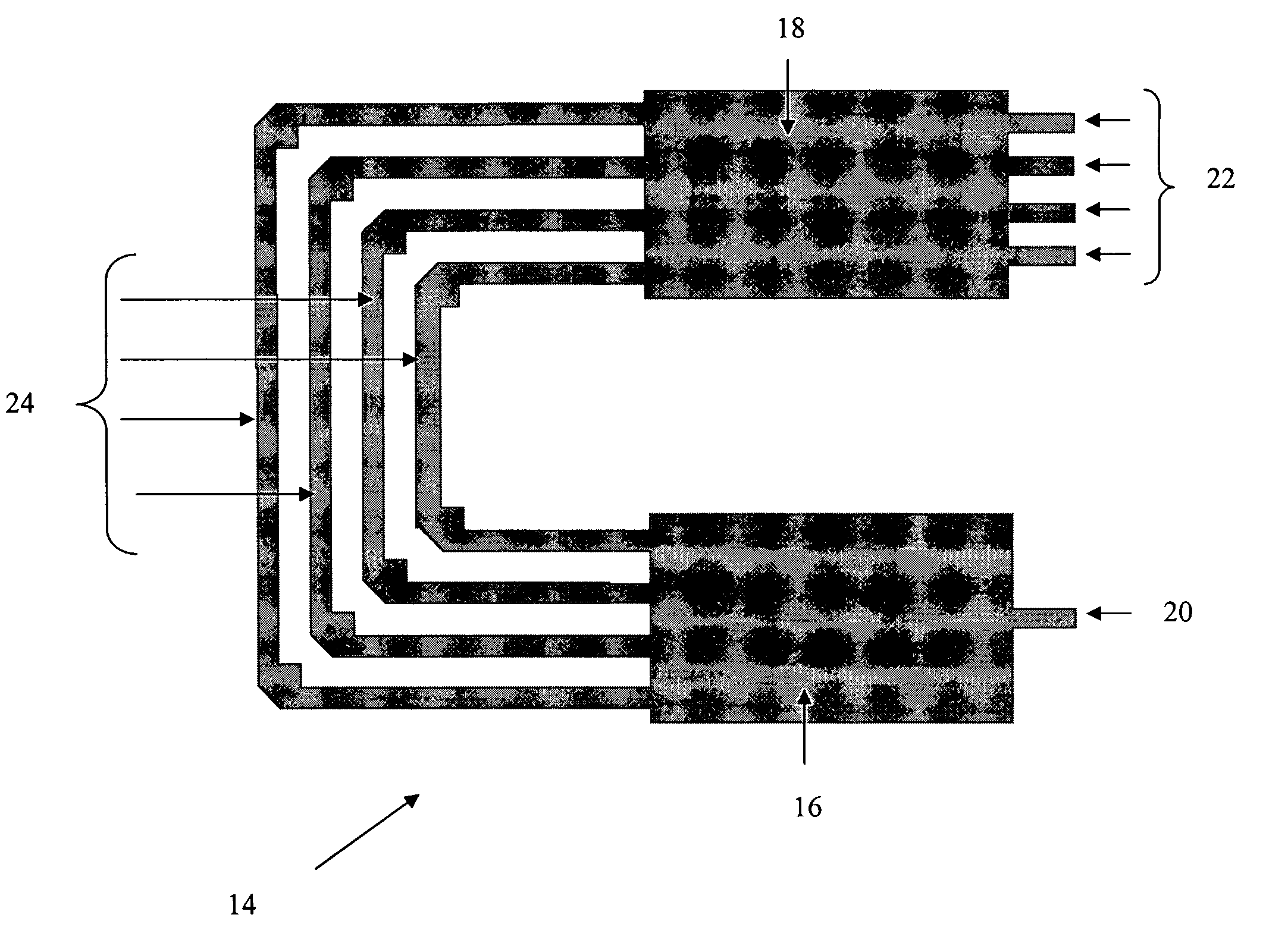
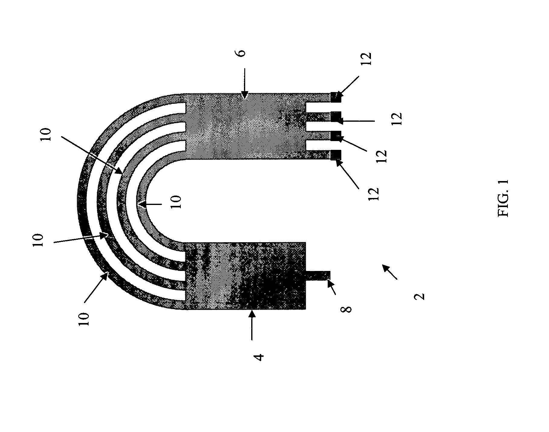
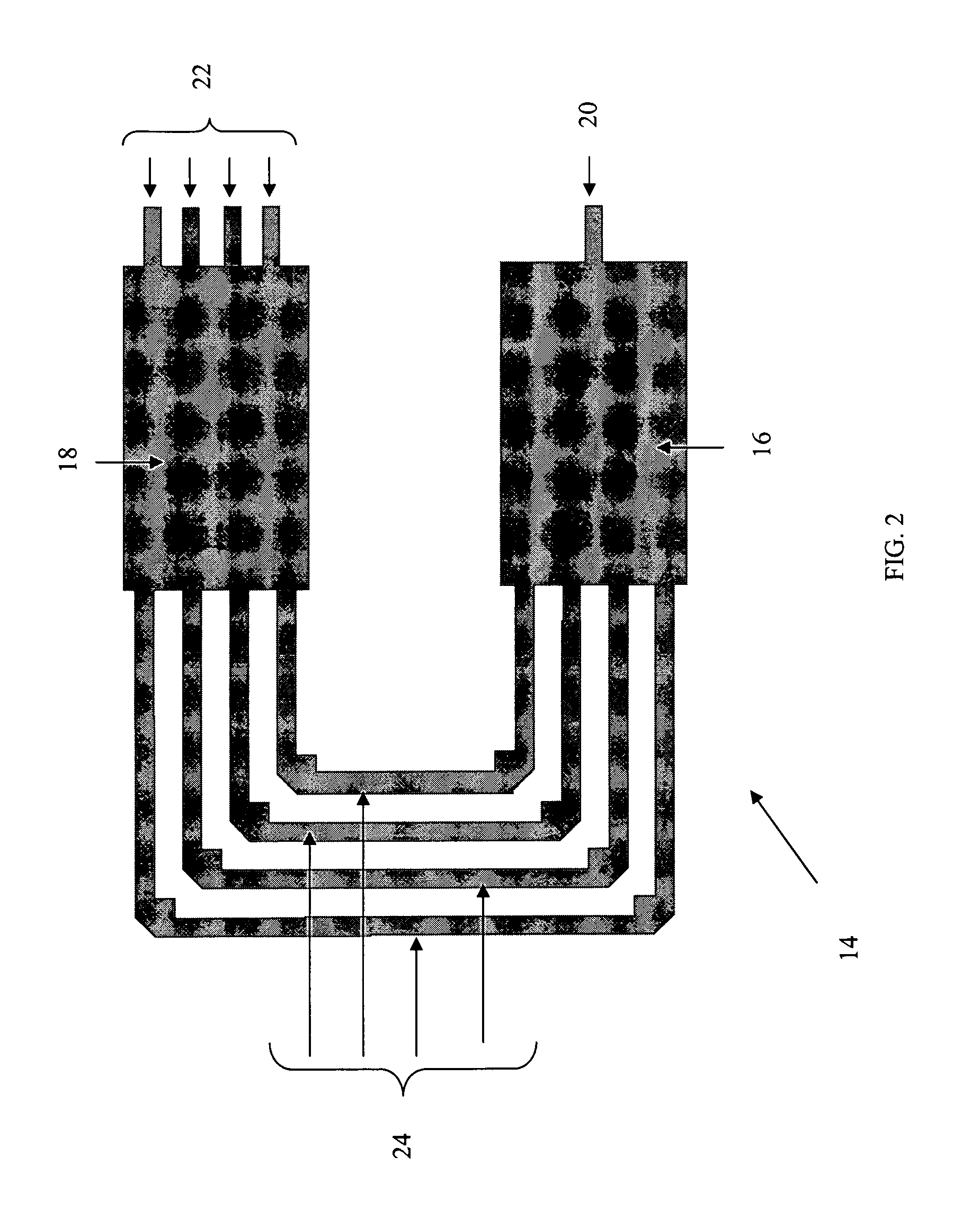
[0013]High index contrast (HIC) structures are a new platform from which to make optical components within a small die area. Typical high index materials include Si and Si3N4, with indices 3.5 and approximately 2.2, respectively. The index contrasts with SiO2 cladding layers are approximately 60 and 40%, respectively.

[0014]The HIC system strongly confines light in the cores, allowing sharp bends, and therefore, small footprints. Having small footprints also enhance the thermal stability because of the negligible expansion of the waveguides. Si and Si3N4 materials are Si IC process compatible. However, sidewall roughness is a crucial factor for low-loss waveguides. Based on the theory to predict the effects of sidewall roughness on light scattering, Si is more sensitive to roughness than is Si3N4 or Si(O)N. However, Si has facet planes, which are atomically flat and can be controlled by post-process annealing. In this way, the sidewall roughness can be controllable.

[0015]For analog s...


PUM


Abstract

An array waveguide grating structure includes an input MMI that receives an input optical signal and splits the optical signal into a plurality of signals, each having a defined wavelength. A plurality of input arrayed waveguide structures receive the plurality of signals such that each of the waveguide structures receives one of the plurality of signals. The input MMI, the plurality of arrayed waveguide structures, and the output waveguide are configured using HIC optics.

Description

PRIORITY INFORMATION[0001]This application claims priority from provisional applications Ser. Nos. 60 / 331,146 filed Nov. 1, 2001 and 60 / 343,346 filed Dec. 21, 2001.BACKGROUND OF THE INVENTION[0002]The invention relates to the field of array waveguide grating, and in particular a high-index-contrast array waveguide grating photonic integrated circuit.[0003]Rapid growth of high-speed, broadband communication has led to a need to increase the capacity of optical communication networks. Wavelength division multiplexing (WDM) systems have key roles in meeting this need. Such networks require a variety of optical components to enable them to directly process light signals. Planar lightwave circuits (PLCs) fabricated using SiO2-based waveguides are employed in various devices. Of the various types of PLCs, arrayed waveguide gratings (AWGs) are superior to other types of wavelength multiplexers / demultiplexers (MUX / DEMUX), such as dielectric multiplayer filters and fiber Bragg gratings in te...

Claims


Application Information

Patent Timeline
Patent Type & Authority Patents(United States)
IPC IPC(8): G02B6/34G02B6/12G02B6/28
CPCG02B6/12007G02B6/12019G02B6/2813G02B2006/12164G02B2006/12109
Inventor WADA, KAZUMIHAUS, HERMANN A.KIMERLING, LIONEL C.
Owner CENT IND SUPPLY
Why Eureka
Try Eureka