Semiconductor Process and Integrated Circuit

a technology of integrated circuits and semiconductors, applied in semiconductor devices, diodes, electrical devices, etc., can solve the problems of inability to successfully utilize the already existing structure to obtain lateral pnp-transistors, high cost, and inability to achieve successful utilization of the already existing structure, etc., to achieve low cost, low processing steps, and high-quality integrated circuits

Inactive Publication Date: 2010-03-04
INFINEON TECH AG
View PDF6 Cites 4 Cited by
  • Summary
  • Abstract
  • Description
  • Claims
  • Application Information

AI Technical Summary

Benefits of technology

[0010]Accordingly, it is an object of the present invention to provide a method in the fabrication of integrated circuits, particularly integrated circuits for radio frequency applications, which provides for effective production of high-quality integrated circuits including bipolar transistors and MOS devices, particularly PMOS-transistors and other p-type MOS devices, by using a minimum of processing steps.
[0023]Still a further object of the present invention is to provide a method in the fabrication of an integrated circuit, particularly an integrated circuit for radio frequency applications, for forming a shallow trench for improved isolation of a vertical bipolar transistor comprised in the circuit.
[0033]Yet a further object of the present invention is to provide an integrated circuit, particularly an integrated circuit for radio frequency applications, including a vertical bipolar transistor, which is isolated by means of a shallow trench in a novel manner, such that an improved performance of the transistor, and thereby the integrated circuit, can be achieved.

Problems solved by technology

It is possible to add high-performing PNP-transistors to the process designed according to the principles described above, but such an approach is usually very costly in terms of additional mask layers and process complexity.
However, when using STI isolation for high-performance RF-IC's, the previously so successful utilization of the already existing structure to obtain a lateral PNP-transistor may not be possible.
Although it is still possible to find the lateral PNP structure, the base now consists mainly of the heavily doped subcollector region, and consequently the current gain (beta) will be too low to be useful.
Furthermore, using the STI isolation of today, problems of leakage current between different device areas may arise.
Besides, it may be difficult to achieve very low base-collector capacitances in the bipolar transistors and a parasitic pnp-device (extrinsic base / n-well / p-well) of high beta, particularly if the n-well has very low doping, may cause problems.

Method used


Image

  • Semiconductor Process and Integrated Circuit
  • Semiconductor Process and Integrated Circuit
  • Semiconductor Process and Integrated Circuit

Examples


Embodiment Construction

[0045]In the following description, for purposes of explanation and not limitation, specific details are set forth in order to provide a thorough understanding of the present invention. However, it will be apparent to one skilled in the art that the present invention may be practiced in other versions that depart from these specific details.

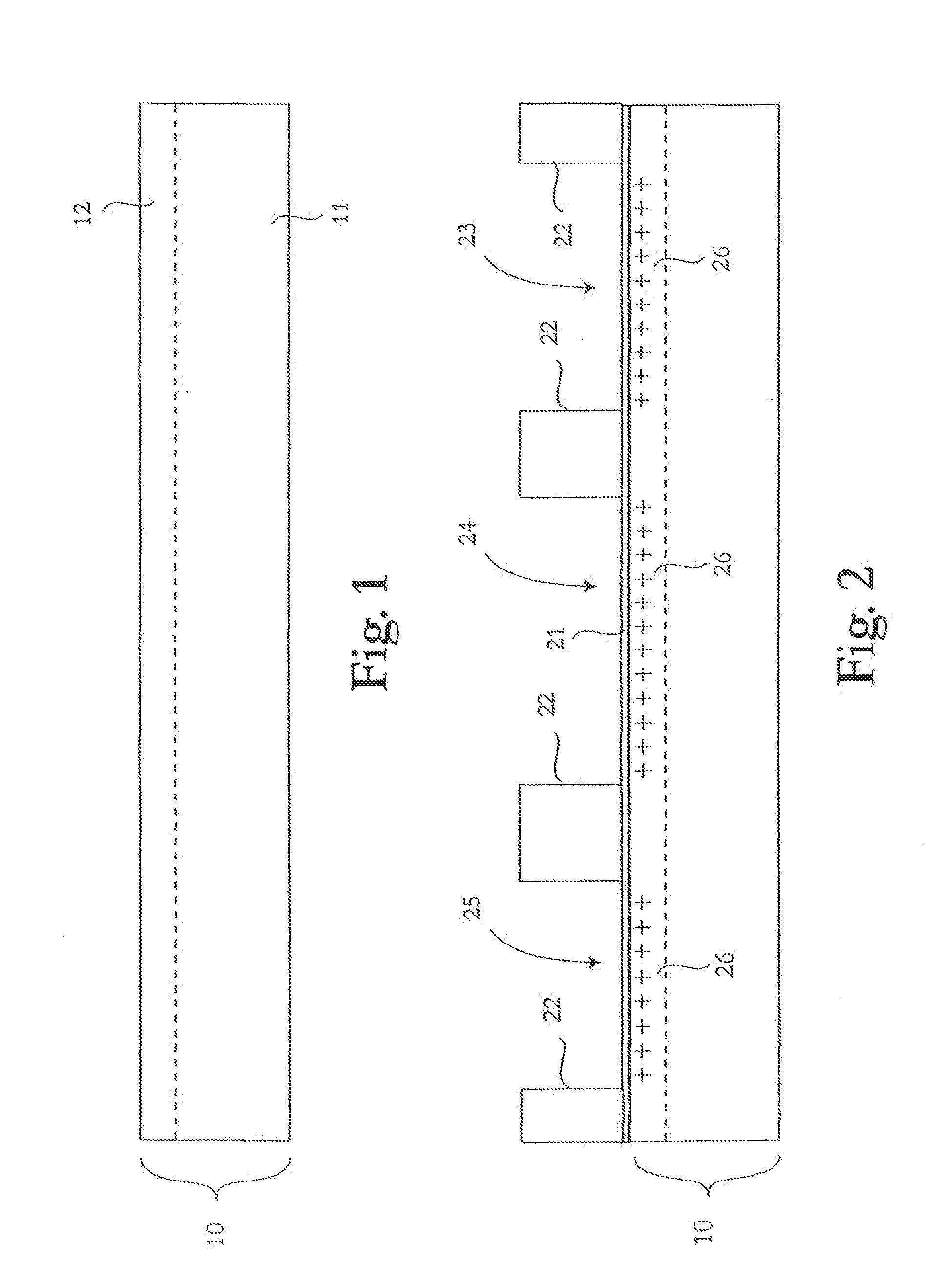
[0046]This description describes a manufacturing method for an integrated silicon bipolar circuit for high frequency applications, including NPN-transistors, nitride and MIM (metal-insulator-metal) capacitors, and resistors. Particularly, the present description illustrates the concept of integrating PMOS transistors into the circuit with the purpose of creating simple p-type of devices, which are necessary for circuit design.

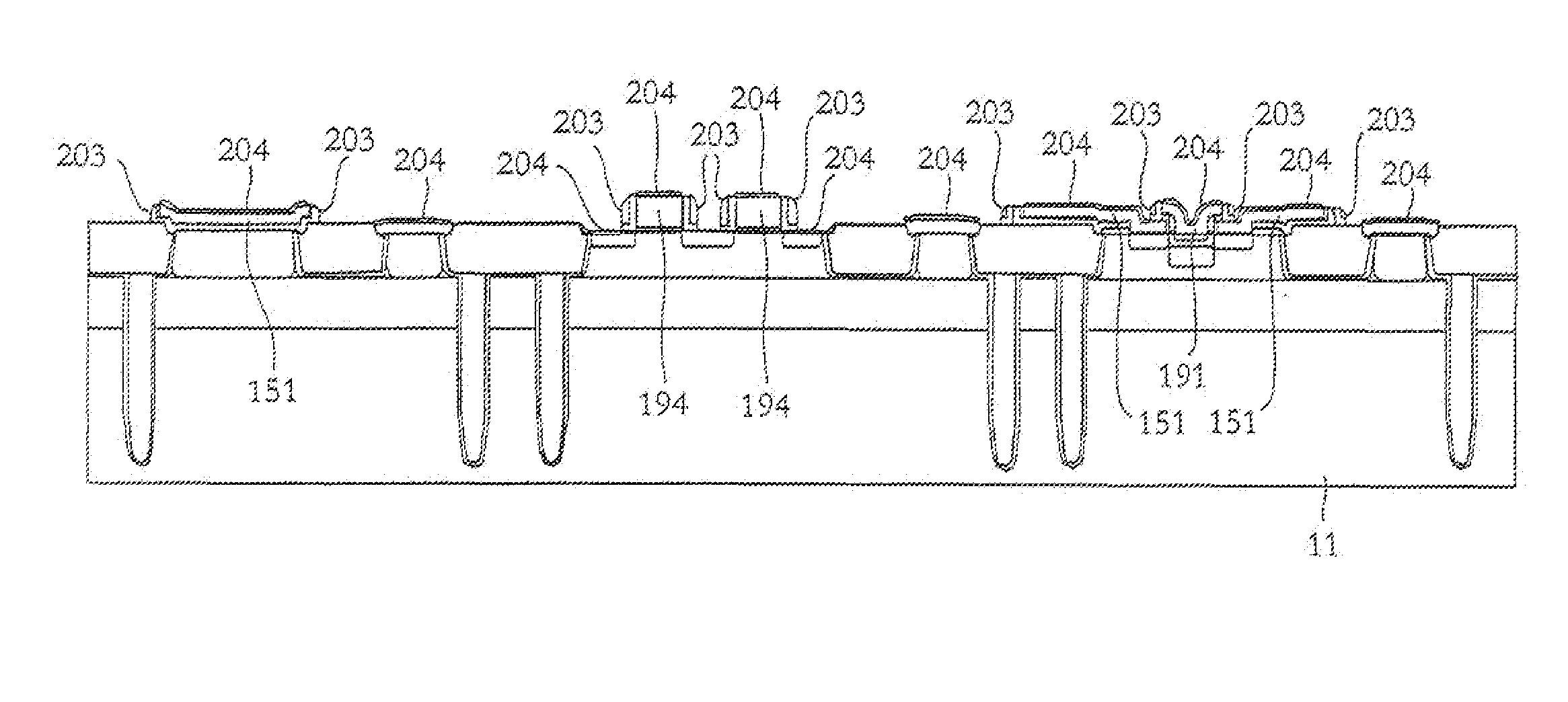
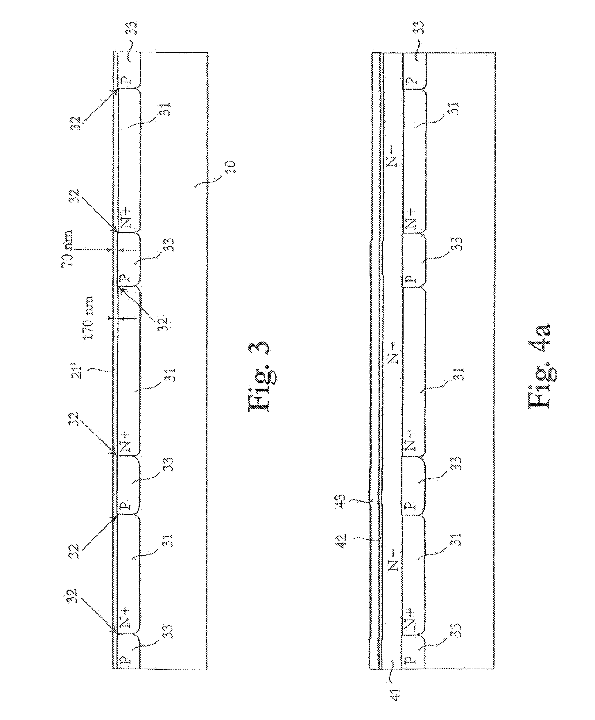
[0047]The importance of selecting a depth of the STI, such that the isolation reaches down to a highly doped subcollector layer, is emphasized.

[0048]Available devices are the following ones:[0049]NPN[0050]PMOS[0051]Quasi-lat...


PUM


Abstract

In the fabrication of an integrated circuit, a shallow trench for isolation of a vertical bipolar transistor comprised in the circuit is fabricated by providing a semiconductor substrate of a first doping type. A buried collector region of a second doping type for the bipolar transistor is formed in the substrate. A silicon layer is epitaxially grown on top of the substrate. An active region of the second doping type for the bipolar transistor is formed in the epitaxially grown silicon layer, the active region being located above the buried collector region. A first trench is formed in the epitaxially grown silicon layer and the silicon substrate, the first trench surrounding, in a horizontal plane, the active region and extending vertically a distance into the substrate. An electrically insulating material is formed in the first trench.

Description

PRIORITY CLAIM[0001]The present application is a divisional of U.S. patent application Ser. No. 10 / 699,222, filed Oct. 31, 2003, which is a continuation of PCT Application No. PCT / SE02 / 00838, filed Apr. 29, 2002, which claims priority to Swedish Application No. 0101567-6, filed May 4, 2001, and Swedish Application No. 0103036-0, filed Sep. 13, 2001, the content each of which is incorporated herein by reference in their entirety.TECHNICAL FIELD OF THE INVENTION[0002]The present invention generally relates to the field of silicon IC-technology, and more specifically to the integration of active and passive devices in a process flow, especially designed for bipolar RF-IC's.BACKGROUND OF THE INVENTION[0003]Advanced silicon bipolar, CMOS or BiCMOS circuits are used today for high-speed applications in the 1-5 GHz frequency range, replacing circuits previously only possible to realize using III-V based technologies. Their major application area is for modern telecommunication systems. The...

Claims


Application Information

Patent Timeline
Patent Type & Authority Applications(United States)
IPC IPC(8): H01L21/331H01L21/762H01L21/76H01L21/822H01L21/8222H01L21/8248H01L21/8249H01L27/04H01L27/06H01L29/732
CPCH01L27/0635H01L21/8249H01L21/18
Inventor JOHANSSON, TEDNORSTROM, HANSALGOTSSON, PATRIK
Owner INFINEON TECH AG
Why Eureka
Try Eureka