Solid-state imaging device and method of producing solid-state imaging device

a solid-state imaging and imaging device technology, applied in the direction of radioation controlled devices, television system scanning details, television systems, etc., can solve the problems of dark current generation, efficient attraction, and achieve sufficient negative band-bending

Inactive Publication Date: 2010-03-11
SONY CORP
View PDF13 Cites 23 Cited by
  • Summary
  • Abstract
  • Description
  • Claims
  • Application Information

AI Technical Summary

Benefits of technology

[0013]In the solid-state imaging device having the above structure, the oxide insulating film containing carbon is provided on the sensor. The oxide insulating film containing carbon functions as a negative-charge accumulation layer having a negative fixed charge. Consequently, by providing the oxide insulating film on the sensor, positive charges can be efficiently attracted to the surface side of the semiconductor substrate by a negative band-bending effect in the oxide insulating film. Consequently, a hole accumulation layer is formed in this portion, thus compensate for the interface state. Furthermore, the amount of negative fixed charge in the oxide insulating film is controlled by the carbon concentration. Accordingly, the hole accumulation layer can be reliably formed on the surface side of the semiconductor substrate by a sufficient band-bending effect.
[0014]As described above, according to the solid-state imaging device according

Problems solved by technology

It is known that, in a solid-state imaging device such as a CCD or CMOS image sensor, crystal defects in the sensor composed of a photodiode a

Method used


Image

  • Solid-state imaging device and method of producing solid-state imaging device
  • Solid-state imaging device and method of producing solid-state imaging device
  • Solid-state imaging device and method of producing solid-state imaging device

Examples


first embodiment

[0024](Embodiment in which Oxide Insulating Film is Composed of Metal Oxide)

[Structure of Solid-State Imaging Device]

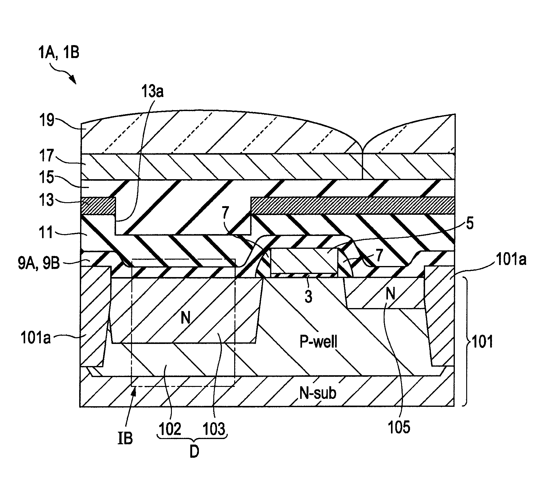
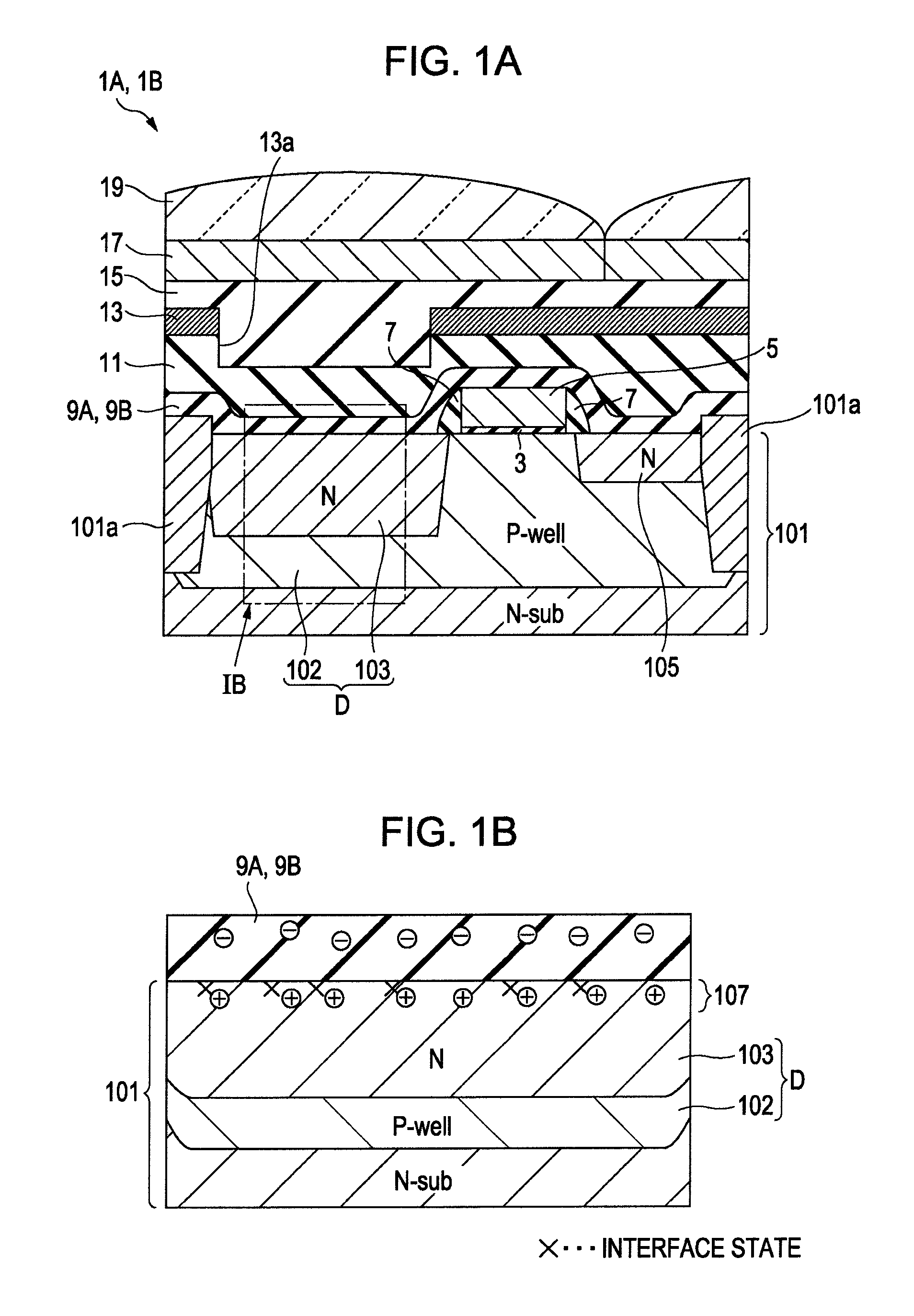
[0025]FIG. 1A is a cross-sectional view of a relevant part of one pixel in the case where a solid-state imaging device according to an embodiment of the present invention is applied to a CMOS sensor. FIG. 1B is an enlarged view of portion IB of FIG. 1A. A solid-state imaging device 1A of a first embodiment shown in FIGS. 1A and 1B has the following structure.

[0026]On a surface side of a semiconductor substrate 101 composed of N-type single-crystal silicon, for example, trench element isolations 101a (shallow trench isolations: STI) are provided to isolate each pixel region. A P-well diffusion layer 102 is provided on the surface side of the semiconductor substrate 101 in each pixel region isolated by the element isolation regions 101a. A transfer gate 5 is pattern-formed on the semiconductor substrate 101 with a gate insulating film 3 therebetween, so as to intersect ...

second embodiment

[0065](Embodiment in which Oxide Insulating Film is Composed of Silicon-Based Material)

[Structure of Solid-State Imaging Device]

[0066]A solid-state imaging device of a second embodiment differs from the solid-state imaging device 1A of the first embodiment described with reference to FIGS. 1A and 1B in the structure of the oxide insulating film, and the other structures of these solid-state imaging devices are the same as each other. The structure of a solid-state imaging device 1B of the second embodiment will now be described with reference to FIGS. 1A and 1B.

[0067]Specifically, in the solid-state imaging device 1B of this second embodiment, a semiconductor substrate 101 including element isolations 101a, a transfer gate 5, a diode D, a floating diffusion portion 105, and transistors constituting a drive circuit is covered with an oxide insulating film 9B composed of a silicon-based material. This oxide insulating film 9B contains carbon, and accordingly, as in the first embodimen...


PUM


Abstract

A solid-state imaging device includes a sensor including an impurity diffusion layer provided in a surface layer of a semiconductor substrate; and an oxide insulating film containing carbon, the oxide insulating film being provided on the sensor.

Description

BACKGROUND OF THE INVENTION[0001]1. Field of the Invention[0002]The present invention relates to a solid-state imaging device and a method of producing a solid-state imaging device. In particular, the present invention relates to a solid-state imaging device in which an interface state of a surface of a semiconductor substrate having a sensor that performs photoelectric conversion can be compensated for.[0003]2. Description of the Related Art[0004]It is known that, in a solid-state imaging device such as a CCD or CMOS image sensor, crystal defects in the sensor composed of a photodiode and an interface state at an interface between a surface of the sensor and a film disposed thereon become causes of generation of dark current. A hole accumulated diode (HAD) structure is known as a technology for suppressing the generation of dark current due to the interface state, which is one of the above causes.[0005]FIG. 8A shows a structure to which the HAD structure is not applied. In the stru...

Claims


Application Information

Patent Timeline
IPC IPC(8): H04N5/335H01L31/18H01L27/146H01L31/10
CPCH01L27/14683H01L27/1463H01L27/146
Inventor OSHIYAMA, ITARUMIYANAMI, YUKIHIYAMA, SUSUMUTANAKA, KAZUKI
Owner SONY CORP
Why Eureka
Try Eureka