Liquid crystal display device

Inactive Publication Date: 2010-03-11
JAPAN DISPLAY CENT INC
View PDF4 Cites 10 Cited by
  • Summary
  • Abstract
  • Description
  • Claims
  • Application Information

AI Technical Summary

Benefits of technology

[0012]Thus, according to one aspect of the invention, there is provided a liquid crystal display device including: an array substrate including pixels arranged in a matrix, a picture electrode provided for each pixel, a scanning line extending in a row direction and a signal line extending in a column direction with an interposed insulation layer; a counter substrate including a common counter electrode for the plurality of pixels, the counter substrate facing the array substrate; a liquid crystal layer including liquid crystal molecules held between the array substrate and the counter substrate, wherein the liquid crystal molecules are aligned substantially in a direction normal to a surface of the substrates under a co

Problems solved by technology

The static electricity may destroy the switching transistors and / or the driver circuits to significantly lower a yield of the liquid crystal display device.
In the case, particularly, that a gate insulation film is formed in a small polycrystalline silicon pattern on the substrate, that long gate electrode leads are formed on the gate insulation film, and that electric capacitors are formed between the polycrystalline silicon patterns and the gate electrode leads, electrostatic destruction may occur between the polycrystalline silicon pattern and the gate electrodes.
In other words, it is highly possibly for the static electricity to destroy the thin-film transistors.
However, since the above conductive materials are not optically transparent, portions of the pixels on which the wiring layers are formed are optically shielded, which results in decrease of brightness of the display.

Method used


Image

  • Liquid crystal display device
  • Liquid crystal display device
  • Liquid crystal display device

Examples


first embodiment

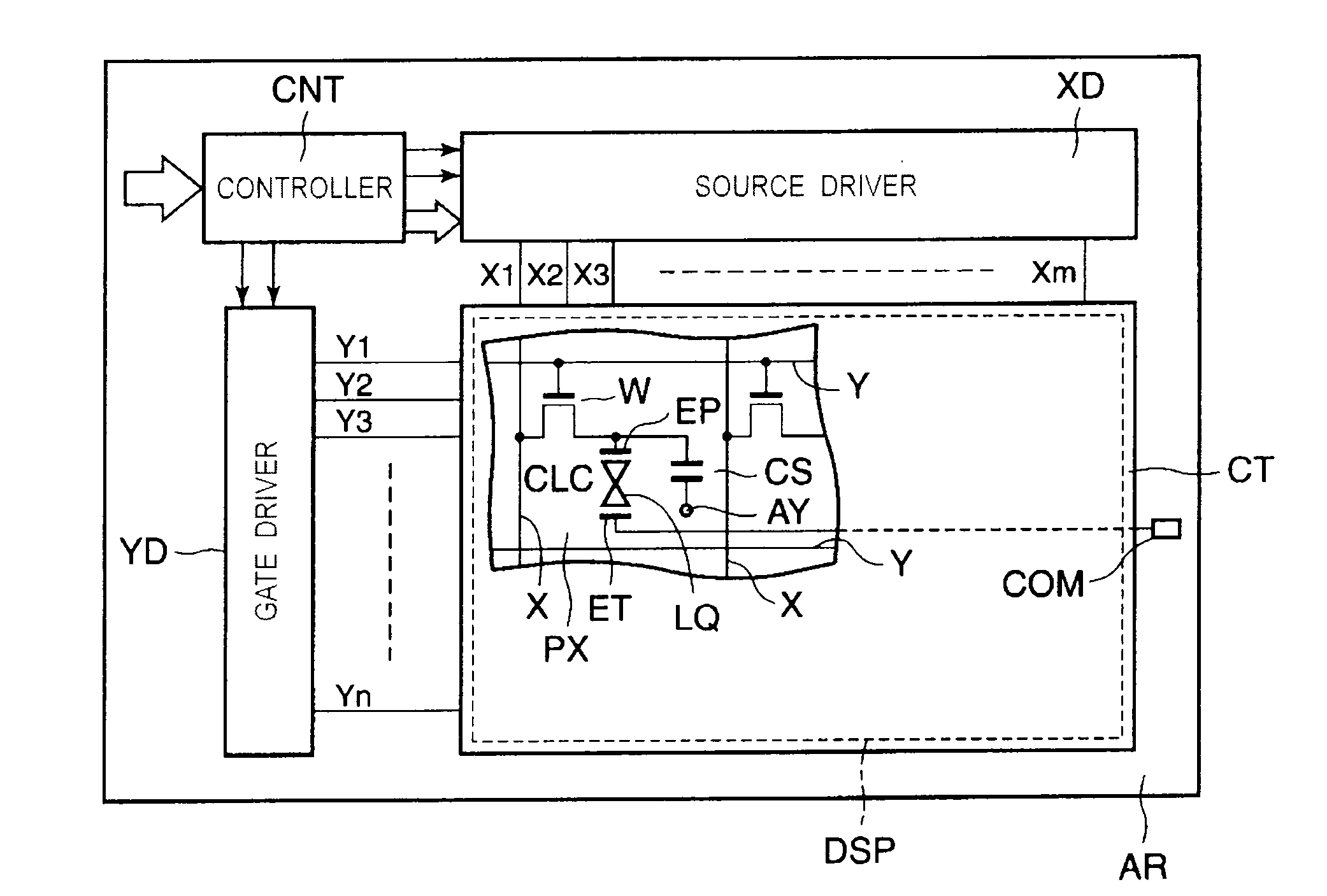
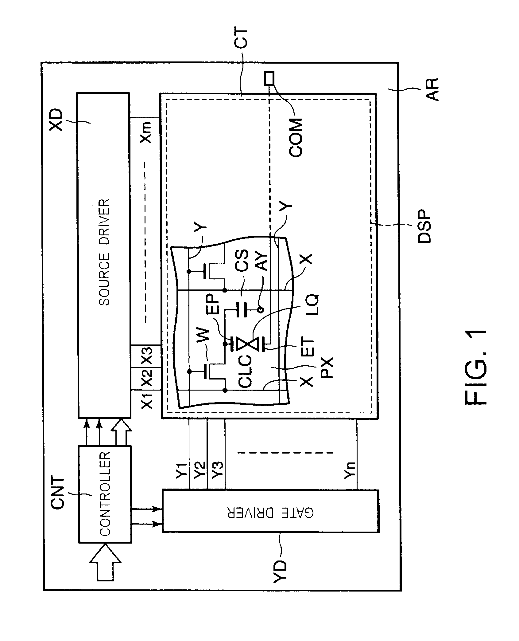
[0031]FIG. 1 and FIG. 2 show a liquid crystal display device of transmissive mode according to the invention, in which pictures are displayed by selectively transmitting light from a backlight unit through a pixel. Of course, the present invention is also applicable to a reflective type liquid crystal display device.

[0032]The liquid crystal display device includes an active matrix type liquid crystal display panel LPN. The liquid crystal display panel LPN includes a pair of electrode substrates, which are an array substrate (first substrate) AR and a counter-substrate (second substrate) CT facing each other and sandwiching a liquid crystal layer LQ which functions as a light modulation layer. The liquid crystal display panel LPN includes an approximately rectangular active area DSP to display pictures. The active area DSP consists of an (m×n) pixels PX arranged in a matrix.

[0033]The liquid crystal display device includes a first optical element OD1 formed on one outer surface of the...

second embodiment

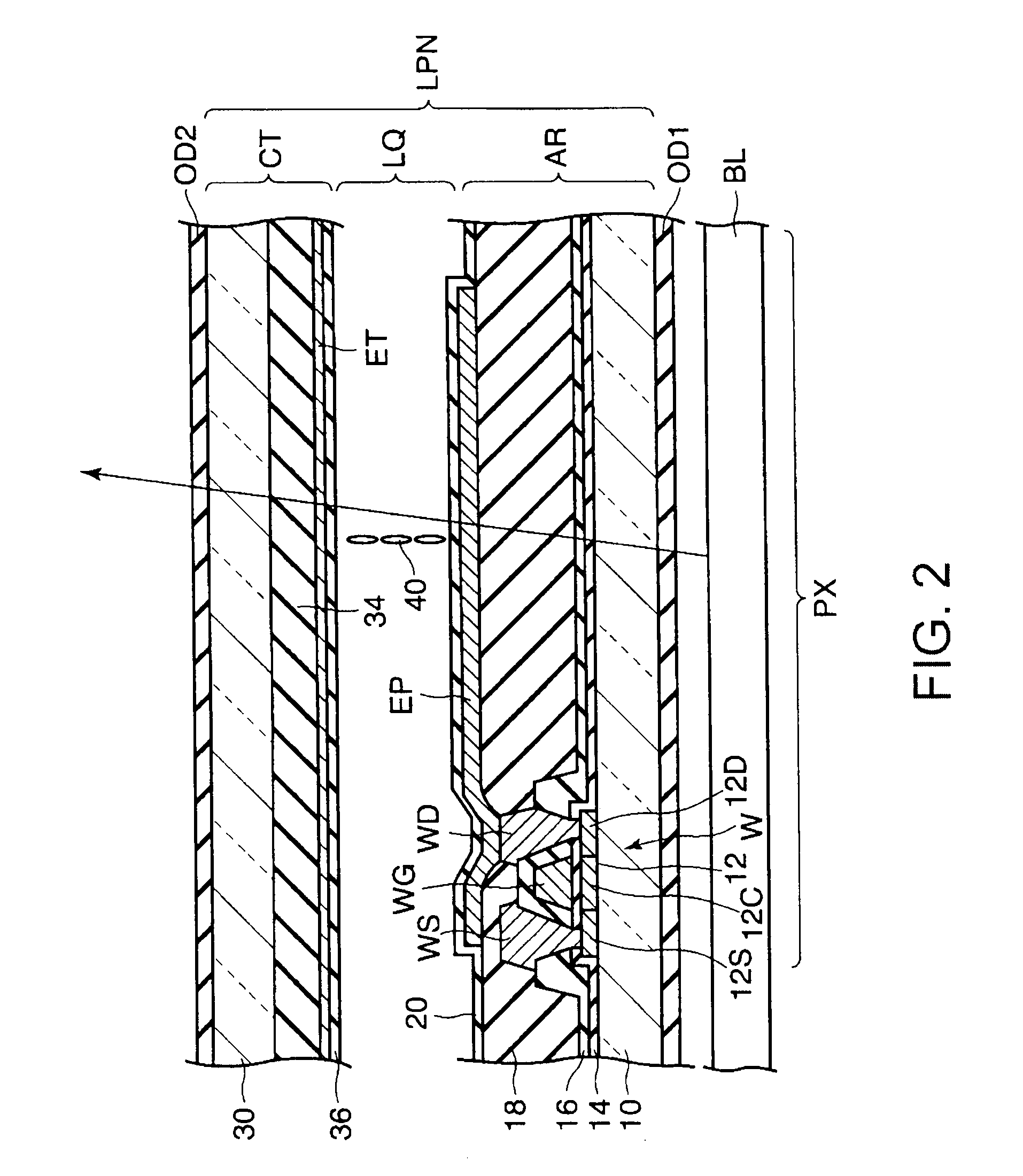
[0073]FIG. 12 and FIG. 13 show a second embodiment according to the invention. The semiconductor layer 12 on the substrate 10 extends under the signal line X with an interposed gate insulation layer 14 and insulation inter layer 16, and crosses the scanning line WG(Y). Then, the semiconductor layer 12 extends, after turning from the signal line X side, to the alignment control device ALC side crossing the pixel. Further, the semiconductor layer 12 extends to a drain electrode WD under the alignment control device ALC. In this embodiment, the semiconductor layer 12 is divided into two segments at a region which is located under the alignment control device ALC so as to separate the semiconductor layer 12 to the scanning line side and the auxiliary capacitance line side to eliminate unfavorable influence from the auxiliary capacitance line AY.

[0074]The first and the second segments S1 and S2 are formed using the same material and the same process, and connected by a second connecting ...

third embodiment

[0080]Next, the invention will be explained referring to FIG. 14 to FIG. 16. In this embodiment, the auxiliary capacitance line AY is divided into two segments so as to disperse a localized concentration of electrostatic charges on the surface of the auxiliary capacitance line AY. The auxiliary capacitance line AY is divided at a region between the alignment control device ALC and the signal line X.

[0081]According to the third embodiment, the auxiliary capacitance line AY includes a first segment AS1 and second segment AS2 apart from each other. The first segment AS1 and the second segment AS2 extend in the row direction H along the periphery of the pixel and face the periphery of the picture electrode EP with the insulation interlayer 16 and the gate insulation layer 14 interposed therebetween. The first segment AS1 and the second segment AS2 are formed on the gate insulation layer 14, and are connected to each other by a third connecting element CN3. The auxiliary capacitance line...


PUM


Abstract

A liquid crystal display device includes an array substrate, a counter substrate and a liquid crystal layer having liquid crystal molecules interposed therebetween. The liquid crystal molecules are aligned in a direction normal to a surface of the substrates under a condition where no electrical voltage is supplied between a picture electrode and a counter electrode. An alignment control device is provided at the counter substrate and configured to control the alignment of the liquid crystal molecules under a condition where an electric field is applied between the picture electrode and the counter electrode. A scanning line crossing a pixel is divided into first and second segments. The array substrate includes a connecting element to connect the first and second segments opposite the alignment control device.

Description

CROSS-REFERENCE TO RELATED APPLICATIONS[0001]This application is based upon and claims the benefit of priority from prior Japanese Patent Application No. 2008-228298 filed Sep. 5, 2008, the entire contents of which are incorporated herein by reference.BACKGROUND OF THE INVENTION[0002]1. Field of the Invention[0003]The present invention relates generally to a liquid crystal display device, and more particularly to a liquid crystal display device of a vertical alignment mode.[0004]2. Description of the Related Art[0005]Liquid crystal display devices are widely used as display devices for various kinds of equipment such as personal computers, OA equipments, and TV sets because the display devices have many advantages such as lightness, compactness and low power consumption. In recent years, the liquid crystal display device has also been used in mobile terminal equipments such as a mobile phone, a car navigation device and a game player.[0006]The liquid crystal display devices include ...

Claims


Application Information

Patent Timeline
IPC IPC(8): G02F1/1337G02F1/1343
CPCG02F1/133707G02F2001/13629G02F1/1393G02F1/136204G02F1/13629
Inventor HARADA, KAZUYUKIKIMURA, HIROYUKI
Owner JAPAN DISPLAY CENT INC
Why Eureka
Try Eureka