Semiconductor package and method of manufacturing the same, and semiconductor device

a semiconductor and semiconductor technology, applied in the direction of printed circuit manufacturing, printed circuit aspects, printed circuit board laminated, etc., can solve the problem of difficult to fit the lead pins with good reliability, and achieve the effect of satisfying mechanical strength

Inactive Publication Date: 2010-03-18
SHINKO ELECTRIC IND CO LTD
View PDF25 Cites 8 Cited by
  • Summary
  • Abstract
  • Description
  • Claims
  • Application Information

AI Technical Summary

Benefits of technology

[0018]As explained above, in the present invention, even when the wiring substrate made thin is employed, a satisfactory mechanical strength can be obtained.

Problems solved by technology

Therefore, according to the equipment and the jig in the prior art, it is difficult to fit the lead pins with good reliability.

Method used


Image

  • Semiconductor package and method of manufacturing the same, and semiconductor device
  • Semiconductor package and method of manufacturing the same, and semiconductor device
  • Semiconductor package and method of manufacturing the same, and semiconductor device

Examples


first embodiment

[0047]FIG. 3 to FIG. 10 are sectional views showing a method of manufacturing a semiconductor package according to a first embodiment of the present invention.

[0048]In the method of manufacturing the semiconductor package according to the first embodiment of the present invention, first, a wiring substrate 10 shown in FIG. 3A is prepared. The wiring substrate 10 shown in FIG. 3A corresponds to one wiring substrate portion B of a large-size substrate 5 for multi production shown in FIG. 3B. In an example of FIG. 3B, five wiring substrate portions and six wiring substrate portions are defined in the lateral direction and the longitudinal direction in the large-size substrate 5 respectively, and individual wiring substrate portions B are obtained by cutting off the large-size substrate in the later step.

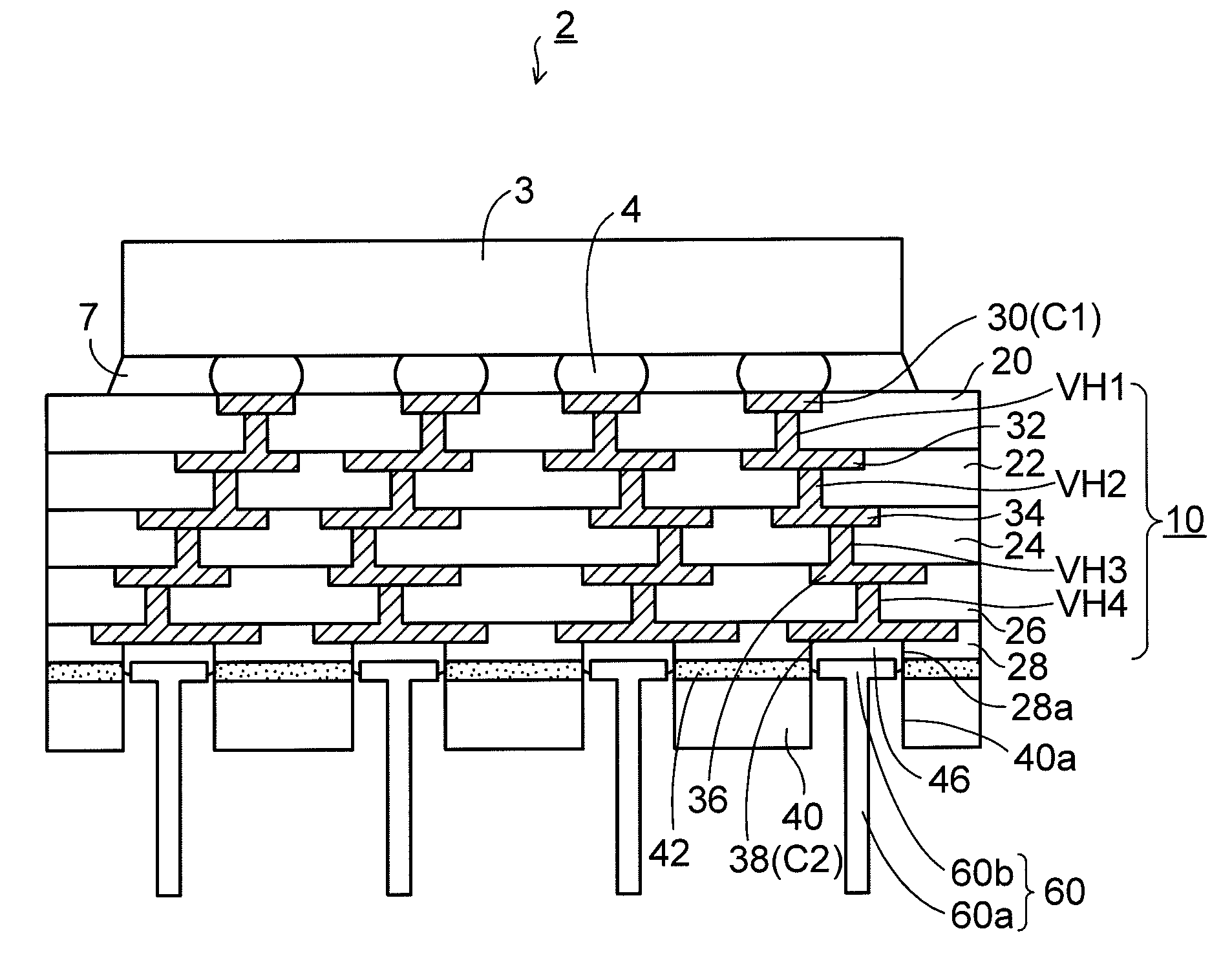
[0049]In the wiring substrate 10 in FIG. 3A, first wiring layers 30 are embedded on the lower portion of a first interlayer insulating layer 20 to expose their lower surfaces thereof, a...

second embodiment

[0116]FIGS. 17A and 17B and FIG. 18 are sectional views showing a method of manufacturing a semiconductor package according to a second embodiment of the present invention. In the second embodiment, the same reference symbols are affixed to the same elements as those in the first embodiment, and their explanation will be omitted herein.

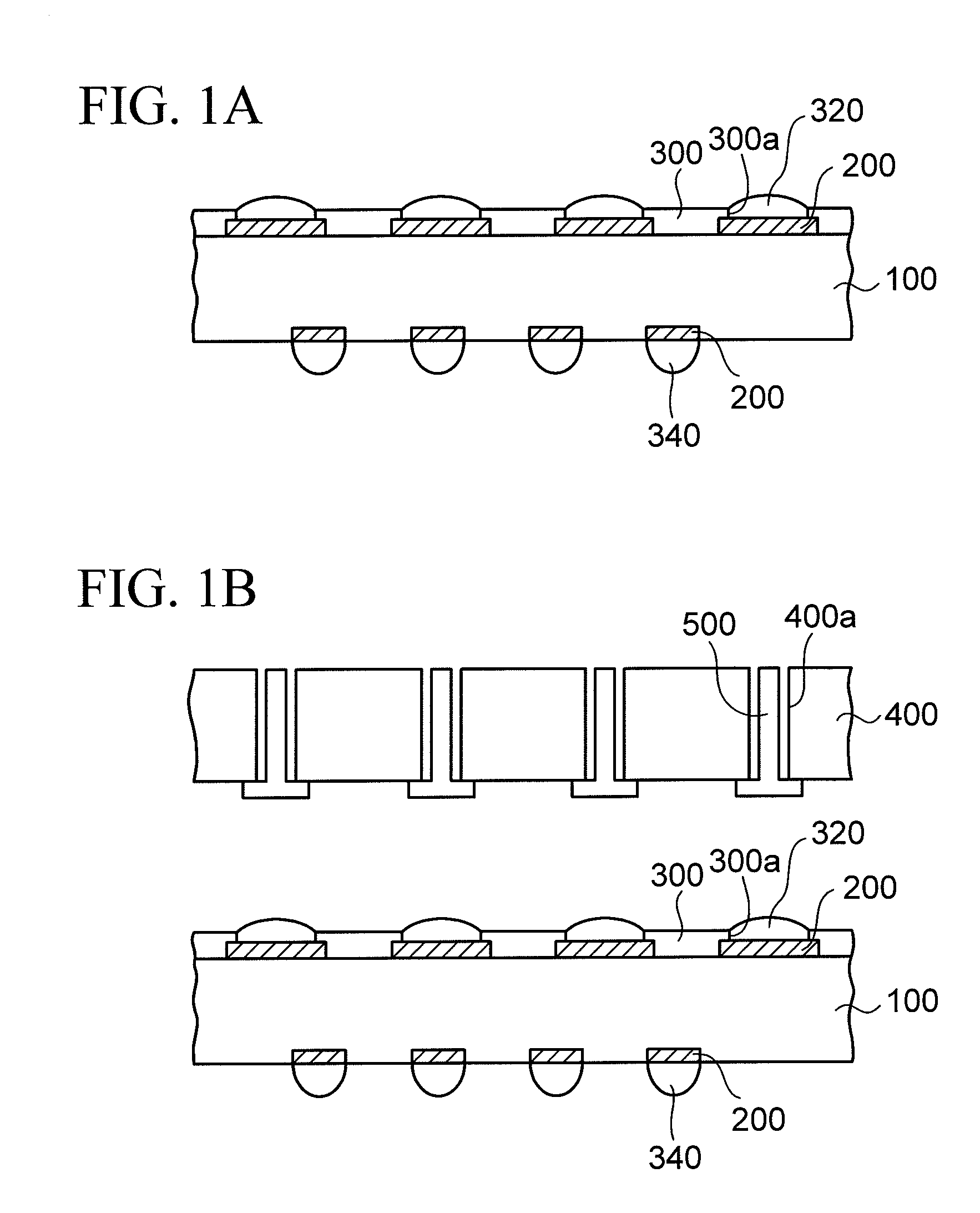
[0117]In the second embodiment, as shown in FIG. 17A, the glass epoxy resin layer 40 (supporting plate) is adhered onto the wiring substrate 10 by the adhesive layer 42 in a state that the wiring substrate 10 is formed on the temporary substrate 11.

[0118]Then, as shown in FIG. 17B, like the steps in FIG. 5 in the above first embodiment, the opening portions 40a are formed on the connection terminal pads C2 by applying the laser processing to the glass epoxy resin layer 40 and the adhesive layer 42.

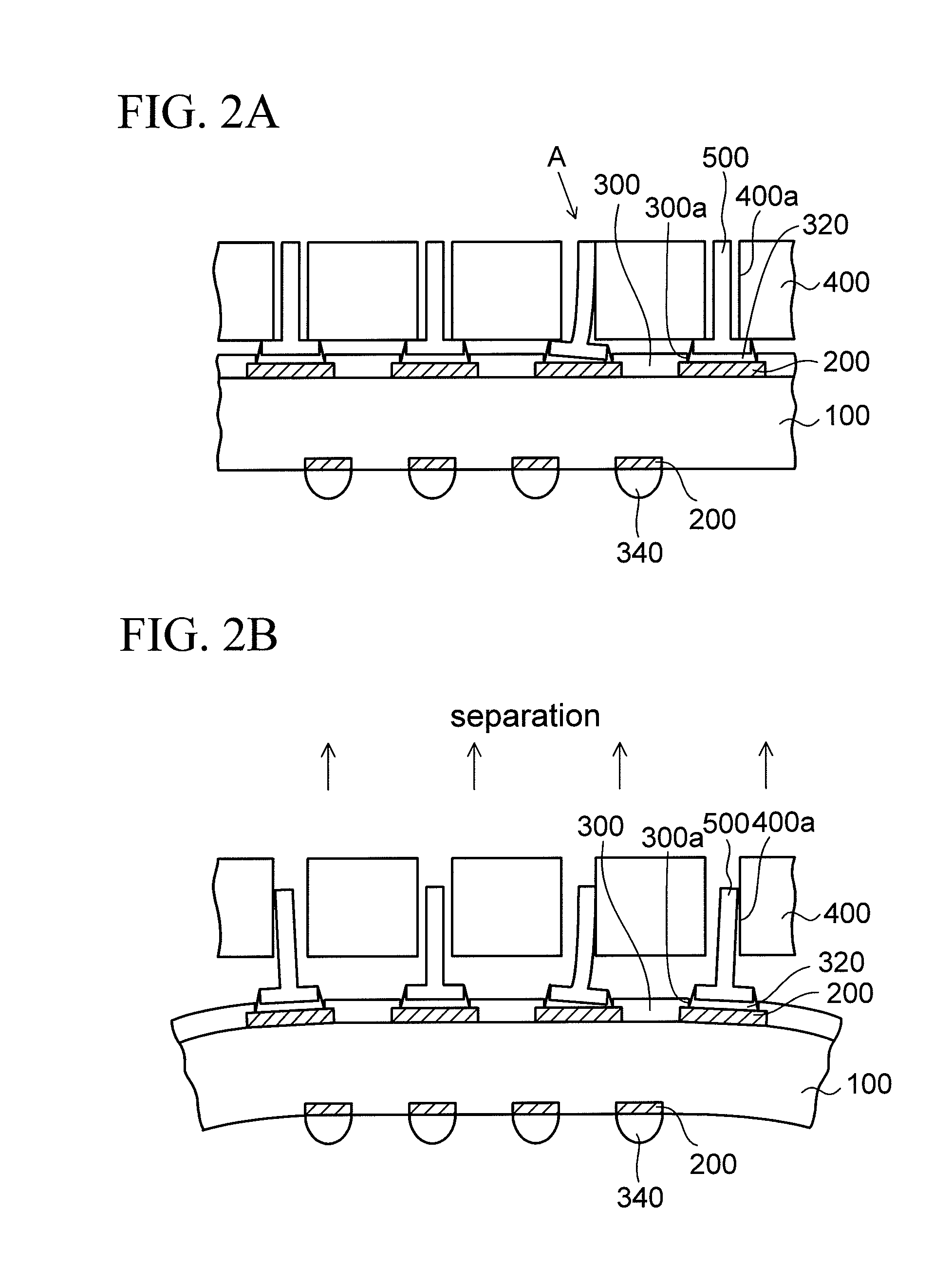
[0119]Then, as shown in FIG. 18, the temporary substrate 11 is removed from the wiring substrate 10. Accordingly, the same structure as that shown in FIG. 5...


PUM


Abstract

A semiconductor package includes a wiring substrate having a connection pad on both surface sides respectively, and a supporting plate provided on one surface side of the wiring substrate and formed of an insulator in which an opening portion is provided in a portion corresponding to the connection pad. The external connection terminals (the lead pins, or the like) are provided on the connection pads on the surface of the wiring substrate on which the supporting plate is provided, and the semiconductor chip is mounted on the connection pads on the opposite surface.

Description

CROSS-REFERENCE TO RELATED APPLICATIONS[0001]This application is based on and claims priority of Japanese Patent Application No. 2008-238798 filed on Sep. 18, 2008, the entire contents of which are incorporated herein by reference.BACKGROUND OF THE INVENTION[0002]1. Field of the Invention[0003]The present invention relates to a semiconductor package on which a semiconductor chip is mounted and a method of manufacturing the same and a semiconductor device.[0004]2. Description of the Related Art[0005]In the prior art, there is the semiconductor package for constructing the semiconductor device by mounting the semiconductor chip. In such semiconductor chip, the semiconductor chip is mounted on one surface of the wiring substrate, and the external connection terminals are provided on the other surface.[0006]In Patent Literature 1 (Patent Application Publication (KOKAI) 2000-323613), such a technology is disclosed that, in the multilayer wiring substrate for the semiconductor device, the...

Claims


Application Information

Patent Timeline
Patent Type & Authority Applications(United States)
IPC IPC(8): H01L23/488H01L23/48H01L21/60H01L21/58
CPCH01L21/6835H05K2203/063H01L23/49816H01L23/49822H01L24/16H01L2221/68345H01L2224/11003H01L2224/16H01L2924/01046H01L2924/01078H01L2924/01079H01L2924/15311H01L2924/15312H05K3/0058H05K3/4682H05K2201/10318H01L23/49811
Inventor HORIUCHI, AKIOYOKOTA, HIROSHI
Owner SHINKO ELECTRIC IND CO LTD
Why Eureka
Try Eureka