

Multilayer ceramic substrate and method for manufacture thereof
- Summary
- Abstract
- Description
- Claims
- Application Information
AI Technical Summary
Benefits of technology
Problems solved by technology
Method used
Image

Examples
example
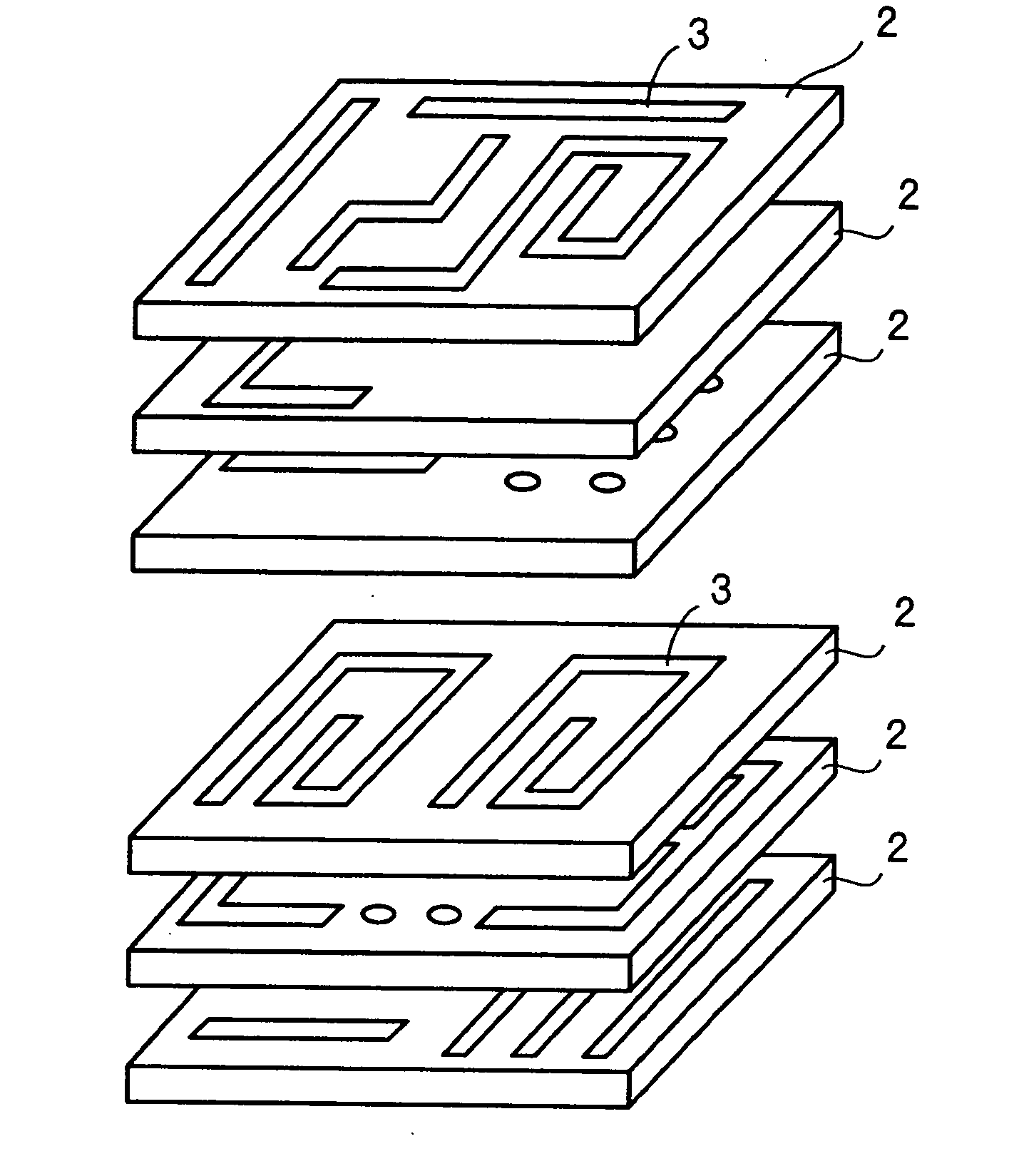
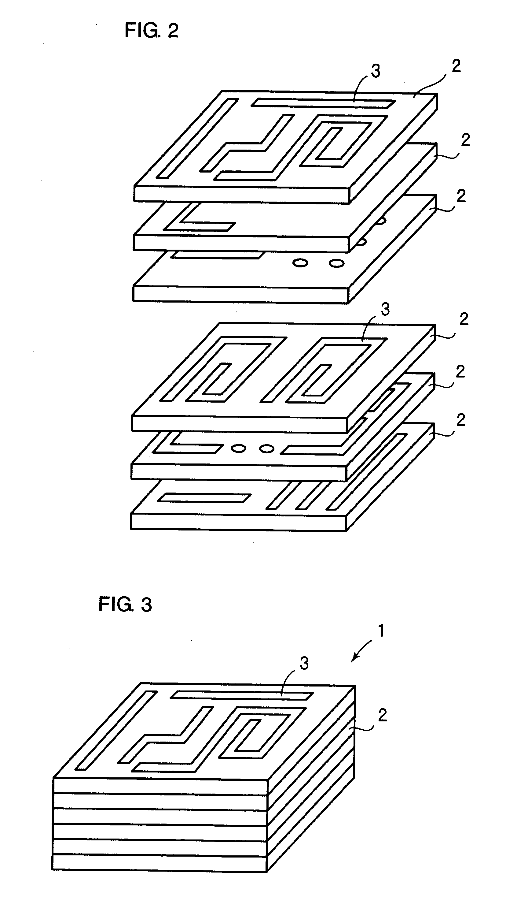
[0052] A ceramic green sheet was prepared by using a low-temperature firable glass-ceramic material containing a Ca-containing amorphous borosilicate glass and alumina in the ratio by weight of (30-60):(70-40). The glass-ceramic material had a composition comprising 44-52% by weight of Al2O3, 33-40% by weight of SiO2, 8.0-13.0% by weight of CaO and 1.0-15.0% by weight of B2O3. The dielectric layer was about 50 μm. The Ag electrode layer was formed on the dielectric layer to a thickness of about 20 μm to prepare the ceramic green sheet.
[0053] Using this ceramic green sheet, a multilayer ceramic substrate shown in FIGS. 2 and 3 was fabricated. Firing was performed according to the firing profiles A1-A3 and B-E, as shown in Table 1 and FIG. 10.
TABLE 1Time081214151717.518.51919.52020.521.523.526.5A2 (Max. Temp. 880° C.)040048268288088083220A1 (Max. Temp. 860° C.)040048268286086083220A3 (Max. Temp. 840° C.)040048268284084083220B040048268286086083220C040048268286086074220D0400482682860...
PUM
| Property | Measurement | Unit |
|---|---|---|
| Grain size | aaaaa | aaaaa |
| Temperature | aaaaa | aaaaa |
| Temperature | aaaaa | aaaaa |
Abstract
Description
Claims
Application Information