Semiconductor integrated circuit, RF module using the same, and radio communication terminal device using the same

a technology of integrated circuits and radio communication terminals, applied in electronic switching, pulse automatic control, pulse technique, etc., can solve the problems of waveform distortion occurring as the transmit power increases, the breakdown voltage is much lower than that of pin diodes, etc., to reduce intermodulation distortion and improve life and operation reliability

Inactive Publication Date: 2010-03-18
RENESAS ELECTRONICS CORP
View PDF9 Cites 35 Cited by
  • Summary
  • Abstract
  • Description
  • Claims
  • Application Information

AI Technical Summary

Benefits of technology

[0104]The effect achieved by a representative embodiment of the invention herein disclosed will be briefly described below.
[0105]That is, the invention can reduce the intermodulation distortion critical for WCDMA system, or the harmonic distortion critical for GSM system in an antenna switch mounted on an RF communication terminal device.
[0106]Further, the effect achieved by a representative embodiment of the invention herein disclosed will be briefly described below.
[0107]That is, the invention can provide a semiconductor IC having a built-in DC boost circuit whose life and operation reliability are improved.

Problems solved by technology

However, the harmonic distortion caused by an antenna switch connected with an output of LPF is emitted into space through the antenna as it is.
However, GaAs switch FETs have the problem that the breakdown voltage is much lower than that of PIN diodes.
Further, in a GaAs monolithic switch IC, a waveform distortion occurs as transmit power increases.

Method used


Image

  • Semiconductor integrated circuit, RF module using the same, and radio communication terminal device using the same
  • Semiconductor integrated circuit, RF module using the same, and radio communication terminal device using the same
  • Semiconductor integrated circuit, RF module using the same, and radio communication terminal device using the same

Examples


Embodiment Construction

Configuration of Mobile Phone

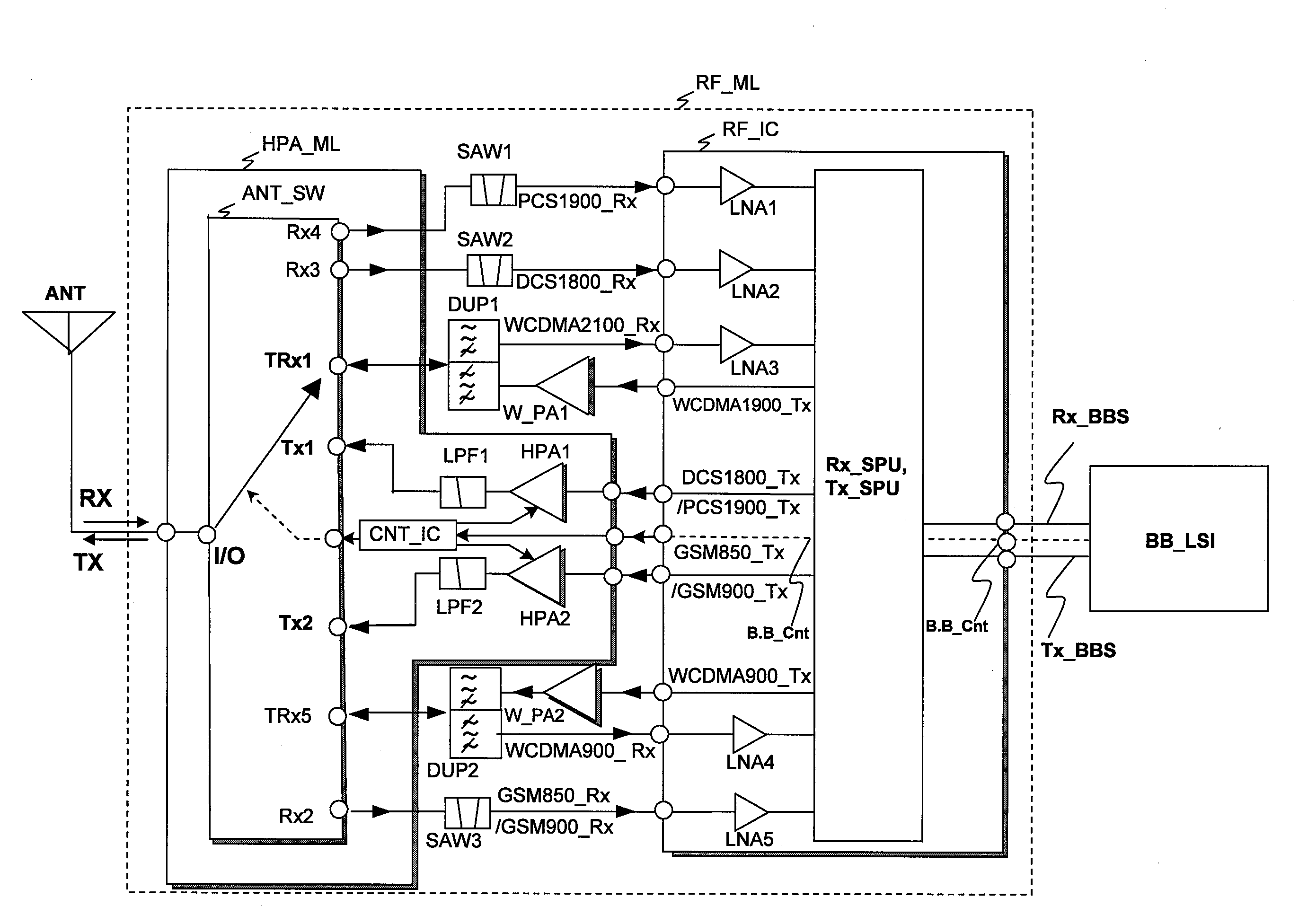
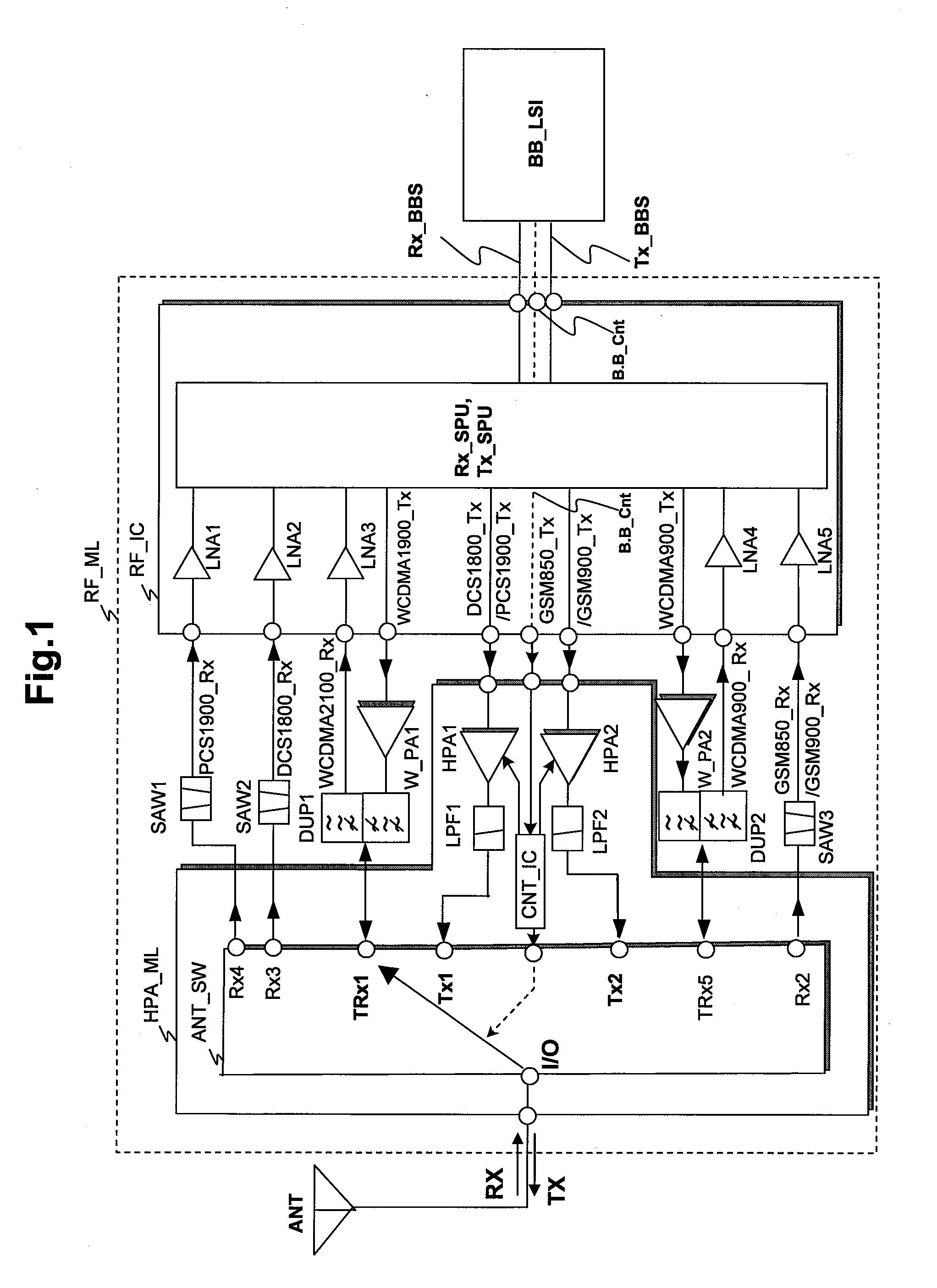
[0125]FIG. 1 is a block diagram showing a configuration of a mobile phone equipped with an RF module incorporating an antenna switch MMIC according to an embodiment of the invention, and a baseband signal processing LSI.

[0126]In the drawing, the mobile phone antenna ANT for transmission and reception is connected to a common input / output terminal I / O of the antenna switch MMIC (ANT_SW) of the RF module RF_ML. A control signal B.B_Cnt from the baseband signal processing LSI (BB_LSI) is passed through an RF analog signal processing semiconductor IC (RF_IC), and supplied to a controller integrated circuit (CNT_IC) of a high-output-power-amplifier module (HPA_ML). A flow of an RF signal from the antenna ANT for transmission and reception to the common input / output terminal I / O leads to a receive operation RX of the mobile phone, and a flow of an RF signal from the common input / output terminal I / O to the antenna ANT for transmission and reception is involved ...


PUM


Abstract

One high-frequency switch Qm supplied with transmit and receive signals to ON, and another high-frequency switch Qn supplied with a signal of another system to OFF are controlled. In the other high-frequency switch Qn, to set V-I characteristics of near-I/O gate resistances Rg1n-Rg3n of a near-I/O FET Qn1 near to a common input/output terminal I/O connected with an antenna are set to be higher in linearity than V-I characteristics of middle-portion gate resistances Rg3n and Rg4n of middle-portion FETs Qn3 and Qn4. Thus, even in case that an uneven RF leak signal is supplied to near-I/O gate resistances Rg1n-Rg3n, and middle-portion gate resistances Rg3n and Rg4n, the distortion of current flowing through the near-I/O gate resistances Rg1n-Rg3n near to the input/output terminal I/O can be reduced.

Description

TECHNICAL FIELD[0001]The present invention relates to a semiconductor IC incorporating a transmitter-receiver switching circuit (antenna switch) for a radio communication system, an RF (Radio Frequency) module incorporating the same, and a radio communication terminal device with the RF module. Particularly, it relates to a technique useful for reducing the intermodulation distortion, which is crucial for WCDMA system, and the harmonic distortion, which is crucial for GSM system.[0002]Also, the invention relates to a semiconductor IC including a DC boost circuit and an RF module incorporating the same, and particularly to a technique useful for increasing the life and operation reliability of devices.BACKGROUND ART[0003]The ubiquitous coverage that wireless communication can be held anywhere in the world, which is an ability of communication terminal equipment, such as mobile phone terminals, has been not a reality today, but under development.[0004]Mobile systems for actualizing th...

Claims


Application Information

Patent Timeline
Patent Type & Authority Applications(United States)
IPC IPC(8): H04B1/44H03K17/687H01P1/10H03L5/00H01P1/15H04B1/3822H04B1/40
CPCH04B1/006H03K17/687H04B1/525H04B1/406
Inventor KOYA, SHIGEKITAKATANI, SHINICHIROOGAWA, TAKASHINAKAJIMA, AKISHIGESHIGENO, YASUSHI
Owner RENESAS ELECTRONICS CORP
Why Eureka
Try Eureka