Method of manufacturing semiconductor chip and semiconductor module

a manufacturing method and technology of semiconductor chips, applied in the direction of individual semiconductor device testing, semiconductor/solid-state device testing/measurement, instruments, etc., can solve the problems of unsuitable commercial criteria, unsuitable commercial criteria, and increase in the manufacturing cost of semiconductor chips/modules, etc., to achieve satisfying electrical performance, satisfying electrical performance, and low cost production

Active Publication Date: 2010-03-25
MITSUBISHI ELECTRIC CORP
View PDF10 Cites 2 Cited by
  • Summary
  • Abstract
  • Description
  • Claims
  • Application Information

AI Technical Summary

Benefits of technology

[0009]The present invention is directed to overcome foregoing problems, and an object thereof is to newly propose an FOM that allows determination from a cost aspect in addition to determination of electrical performance and to provide a method of manufacturing, based on the FOM, a semiconductor chip and a semiconductor module at lower cost in addition to satisfying electrical performance.
[0012]According to the present invention, there is provided a method of manufacturing a semiconductor chip intended for a lower cost production, in addition to satisfying electrical performance.

Problems solved by technology

However, even though the semiconductor chip or semiconductor module that satisfies desired performance is designed and manufactured based upon the FOM, such production process does not necessarily result in commercially successful products.
For instance, even if desired performance is satisfied, a manufacturing cost of semiconductor chip / module may in fact rise.
In this way, the FOM can be used to determine performance of the semiconductor chip or the semiconductor module, but cannot be used as commercial criteria.

Method used


Image

  • Method of manufacturing semiconductor chip and semiconductor module
  • Method of manufacturing semiconductor chip and semiconductor module

Examples


Embodiment Construction

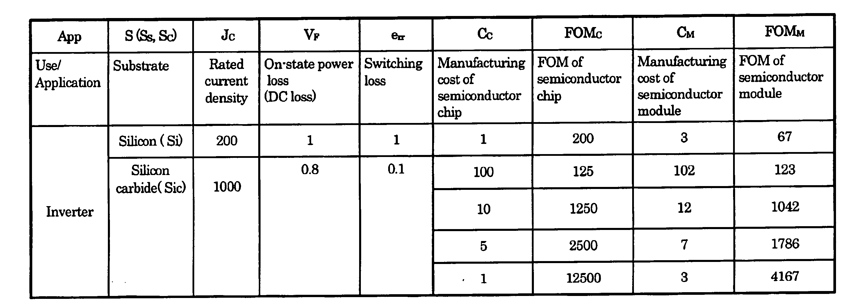
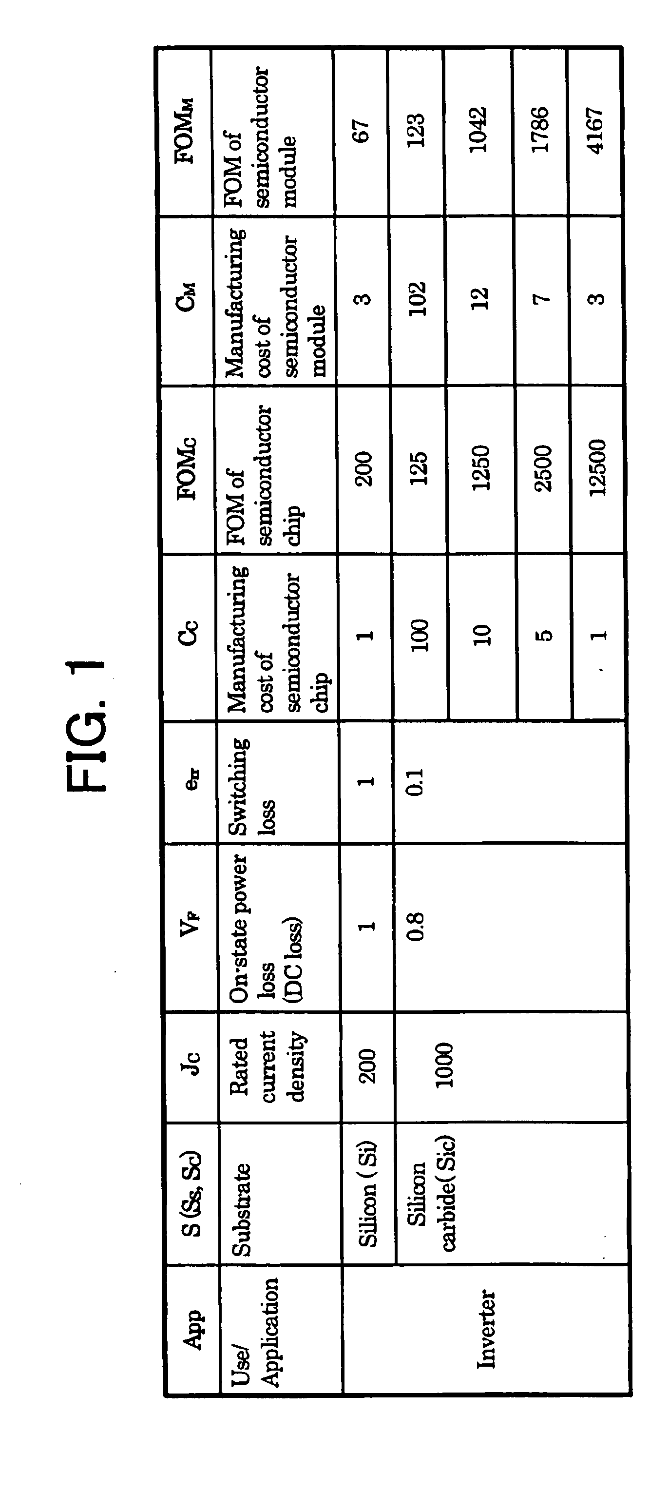
[0015]To start with, an FOM according to the present invention is shown as Equation 1.

FOM=Jc / (VF×err×C)   Equation 1

where JC represents a rated current density (A / cm2); VF, an on-state power loss (DC power loss); and err, a switching loss, with each symbol showing an electrical characteristic and C also denoting a manufacturing cost of semiconductor chip CC or the manufacturing cost of a semiconductor module CM. As is evident from Equation 1, the FOM is defined as the product of a term JC / (VF×err×C) represented by electrical performance and a term 1 / C represented by either of the costs.

[0016]FIG. 1 shows an example of a result of applying to an inverter the FOB shown in Equation 1.

[0017]Referring to FIG. 1 (table), a column labeled App shows an application, i.e., an objective product, where is assumed an inverter; a type of a substrate labeled S is shown which is applied to the applicable product, where a silicone (Si) substrate SS and a silicon carbide (SiC) substrate SC are applie...


PUM


Abstract

An FOM (figure of merit) enabling evaluation from a cost aspect, as well as evaluation of electrical performance, is newly proposed to provide a method of manufacturing based on the FOM a semiconductor chip intended for a lower cost production in addition to satisfying electrical performance. An FOMC of a semiconductor chip is defined as the product of a term represented by electrical performance of a substrate S and a term represented by a semiconductor chip cost CC; the FOMC of each of the semiconductor chips on substrates SS, SC of different type is determined by calculation of the product thereof. Based on the magnitudes of the calculation results, a desired substrate is selected from the substrates SS, SC and then a semiconductor chip is fabricated by forming a semiconductor element on the desired substrate selected.

Description

FIELD OF THE INVENTION[0001]The present invention relates to methods of manufacturing semiconductor chips and semiconductor modules.BACKGROUND OF THE INVENTION[0002]A performance index called an FOM (figure of merit) is employed to determine the performance of a semiconductor chip or a semiconductor module having a plurality of semiconductor chips therein.[0003]The FOM is represented by an equation incorporating electrical characteristics of on-resistance, charge density, and the like in order to determine the electrical performance of a semiconductor chip or a semiconductor module. By using a value of an FOM gained by substituting a specific value of the electrical characteristic into the FOM equation, individual performance of the semiconductor chip or the semiconductor module is determined, or performance of one chip / module is compared with that of another semiconductor chip / module.[0004]For instance, Japanese Unexamined Patent Publication No. 2000-156503 (paragraph 0006) disclos...

Claims


Application Information

Patent Timeline
Patent Type & Authority Applications(United States)
IPC IPC(8): H01L21/66H01L21/50
CPCG06Q10/06H01L29/1608G06Q50/04Y02P90/30
Inventor ARAI, KIYOSHIGOURAB, MAJUMDAR
Owner MITSUBISHI ELECTRIC CORP
Why Eureka
Try Eureka