Semiconductor device

a technology of semiconductors and devices, applied in the direction of semiconductor devices, basic electric elements, electrical equipment, etc., can solve the problems of insufficient suppression, and achieve the effect of reducing reverse leakage current and maintaining forward characteristics

Active Publication Date: 2010-04-01
SANKEN ELECTRIC CO LTD
View PDF7 Cites 32 Cited by
  • Summary
  • Abstract
  • Description
  • Claims
  • Application Information

AI Technical Summary

Benefits of technology

[0018]The invention can provide a semiconductor device which can not only maintain forward characteristics in the forward operation but also reduce the reverse leakage current.

Problems solved by technology

The large reverse leakage current can be reduced by selectively using a transition metal such as platinum (Pt) or rhodium (Rh) as an electrode material for the anode electrode, but cannot be suppressed sufficiently.

Method used


Image

  • Semiconductor device
  • Semiconductor device
  • Semiconductor device

Examples


first embodiment

Features of First Embodiment

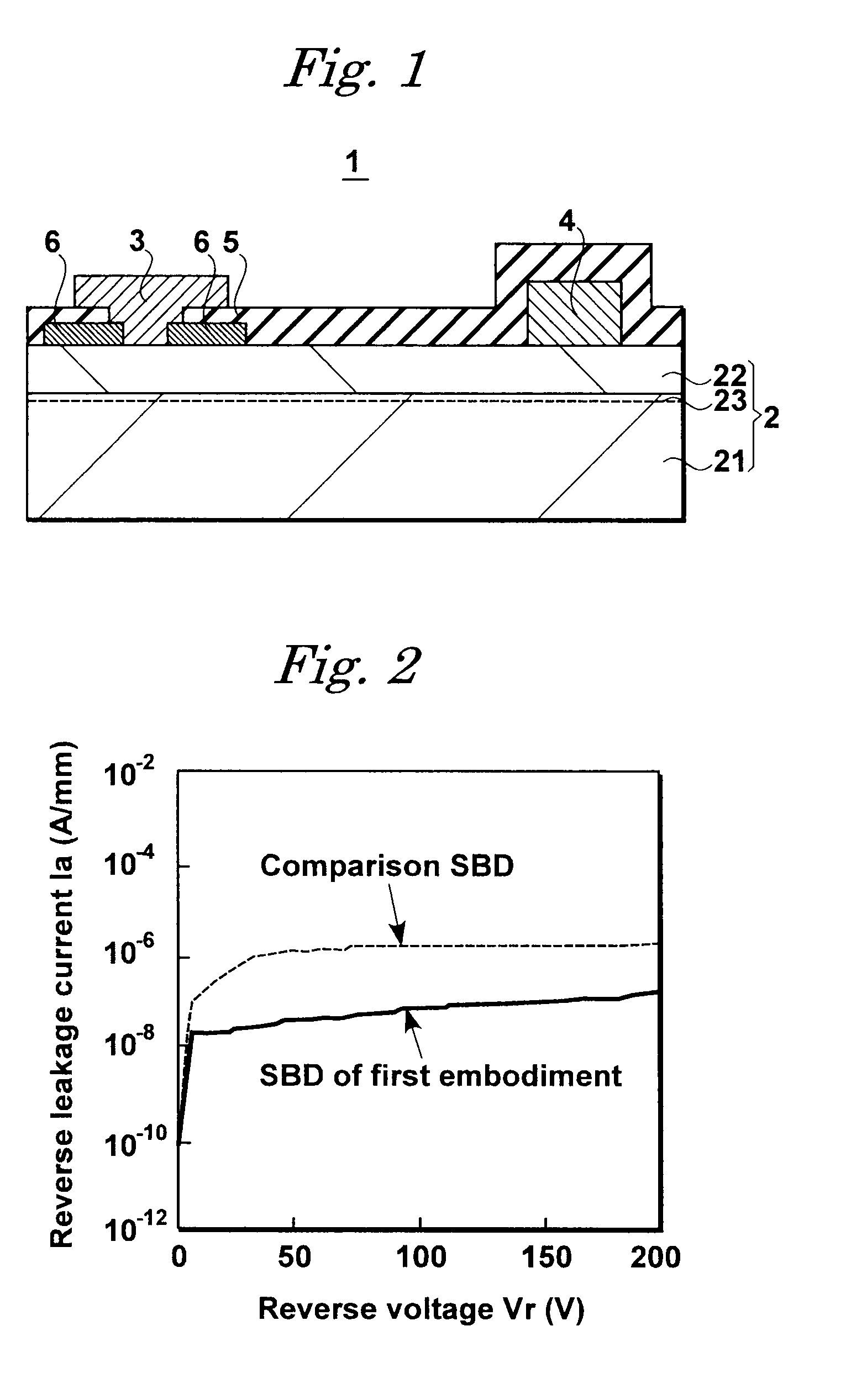
[0044]Reverse characteristics of the horizontal SBD 1 are shown in FIG. 2, in which the abscissa denotes a reverse voltage Vr while the ordinate denotes a leakage current Ia. The reverse leakage current Ia of the horizontal SBD 1 of the invention can be reduced by single digit figure or more compared to the leakage current Ia of a comparison example which does not have metal oxide films 6.

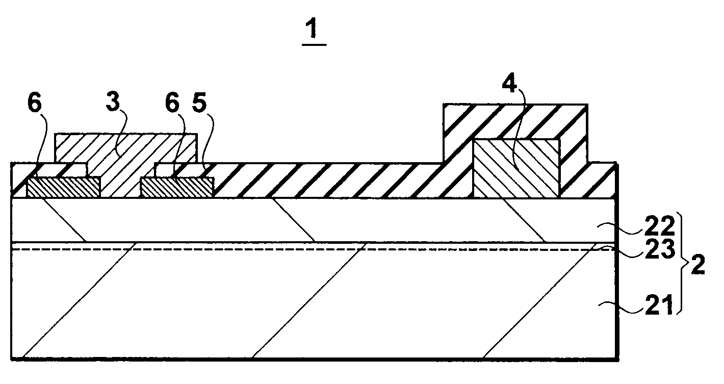
[0045]The horizontal SBD 1 of the first embodiment can reduce the reverse leakage current while it relatively maintains the forward characteristics in the forward operation. This is because the horizontal SBD 1 is provided with the metal oxide films 6 between the first and second main electrode 3 and 4, and the carrier density of the two-dimensional carrier gas layer 23 immediately under the metal oxide films 6 can be reduced.

first modified example

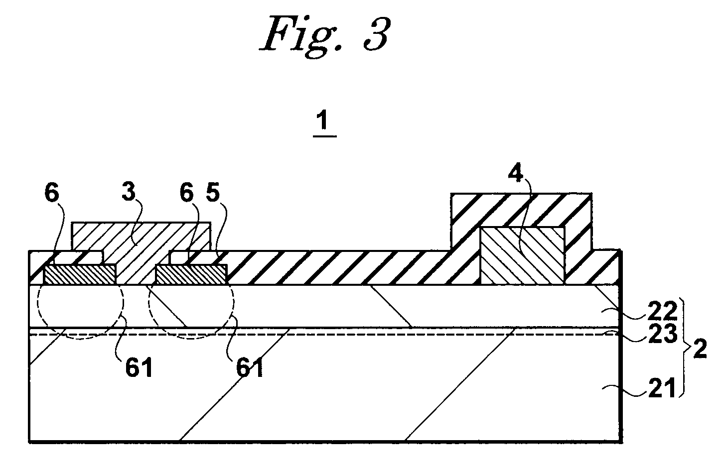
[0046]Referring to FIG. 3, a horizontal SBD 1 of a first modified example produces depletion layers 61 from an interface of the metal oxide films 6 and the second nitride group semiconductor region 22 to the nitride group semiconductor functional layer 2. In other words, the depletion layers 61 extend to or preferably across the two-dimensional carrier gas layer 23. In the latter case, the two-dimensional carrier gas layer 23 is completely depleted at one end of the first main electrode 3 and just under the metal oxide films 6. Therefore, the first main electrode 3 may be an ohmic electrode similarly to the second main electrode 4. In such a case, the on-state voltage can be lowered.

[0047]In the first modified example, the horizontal SBD 1 can reduce the reverse leakage current while it relatively maintains the forward characteristics in the forward operation. This is because the horizontal SBD 1 includes the metal oxide films 6, and the depletion layers 61 produced from an interfac...

second modified example

[0048]In a second modified example shown in FIG. 4(a), a horizontal SBD 1 has recesses 24 extending from the surface of the second nitride group semiconductor region 22 to the two-dimensional carrier gas layer 23, and metal oxide films 6 which extend from the second nitride group semiconductor region 22 and are positioned in the recesses 24 (on sides or bottoms thereof). The recesses 24 are made by scraping the surface of the secondary nitride group semiconductor region 22, and effectively shorten an effective distance between the metal oxide films 6 and the two-dimensional carrier gas layer 23. Since the metal oxide films 6 are buried in the recesses 24, the depletion layers 61 can easily cross the two-dimensional carrier gas layer 23 during the reverse operation. Further, the recesses 24 are made on the secondary nitride group semiconductor region 22 and do not to reach the upper surface of the first nitride group semiconductor region 21 where the two-dimensional carrier gas layer...


PUM


Abstract

A semiconductor device include: a nitride group semiconductor functional layer including a second nitride group semiconductor region on a first nitride group semiconductor region where a two-dimensional carrier gas layer is made, the second nitride group semiconductor region functioning as a barrier layer; a first main electrode electrically connected to one end of the two-dimensional carrier gas layer; a second main electrode electrically connected to the other end of the two-dimensional carrier gas layer; and metal oxide films placed between the first and second main electrodes, electrically connected to the first main electrode, and reducing a carrier density of the two-dimensional carrier gas layer.

Description

CROSS REFERENCE TO RELATED APPLICATION[0001]This application is based upon and claims the benefit of priority from the prior Japanese Patent Application No. 2008-255.232 filed on Sep. 30, 2008, the entire contents of which is incorporated herein by reference.BACKGROUND OF THE INVENTION[0002]1. Field of the Invention[0003]The present invention relates to a semiconductor device, and more particularly to a semiconductor device which includes a nitride group functional semiconductor layer having a two-dimensional carrier gas layer near a hetero junction.[0004]2. Description of the Related Art[0005]Horizontal Shottky barrier diodes (SBD) are well-known, and have a hetero junction structure constituted by gallium nitride (GaN) and aluminum gallium nitride (AlGaN). Such a horizontal SBD is fabricated as a nitride group functional semiconductor layer having a GaN layer and an AlGaN layer placed on the GaN layer by the hetero junction. The SBD also includes not only a two-dimensional electro...

Claims


Application Information

Patent Timeline
Patent Type & Authority Applications(United States)
IPC IPC(8): H01L29/772
CPCH01L29/2003H01L29/872H01L29/402H01L29/205
Inventor BABA, RYOHEIIWAKAMI, SHINICHI
Owner SANKEN ELECTRIC CO LTD
Why Eureka
Try Eureka