Substrate for liquid crystal display device

Inactive Publication Date: 2010-04-01
FUJIFILM CORP
View PDF0 Cites 2 Cited by
  • Summary
  • Abstract
  • Description
  • Claims
  • Application Information

AI Technical Summary

Benefits of technology

[0009]The object of the present invention is to provide a substrate for liquid crystal display devic

Problems solved by technology

Further, the dimensions of the retardation film vary with temperat

Method used


Image

  • Substrate for liquid crystal display device
  • Substrate for liquid crystal display device
  • Substrate for liquid crystal display device

Examples


example 1

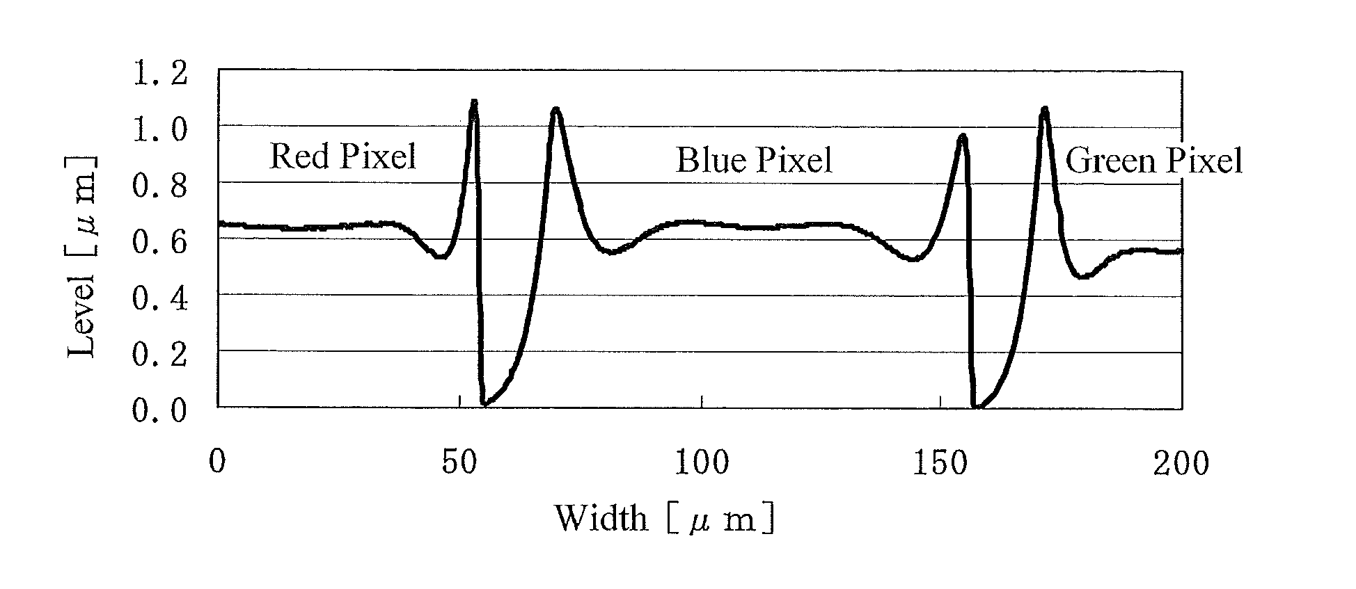
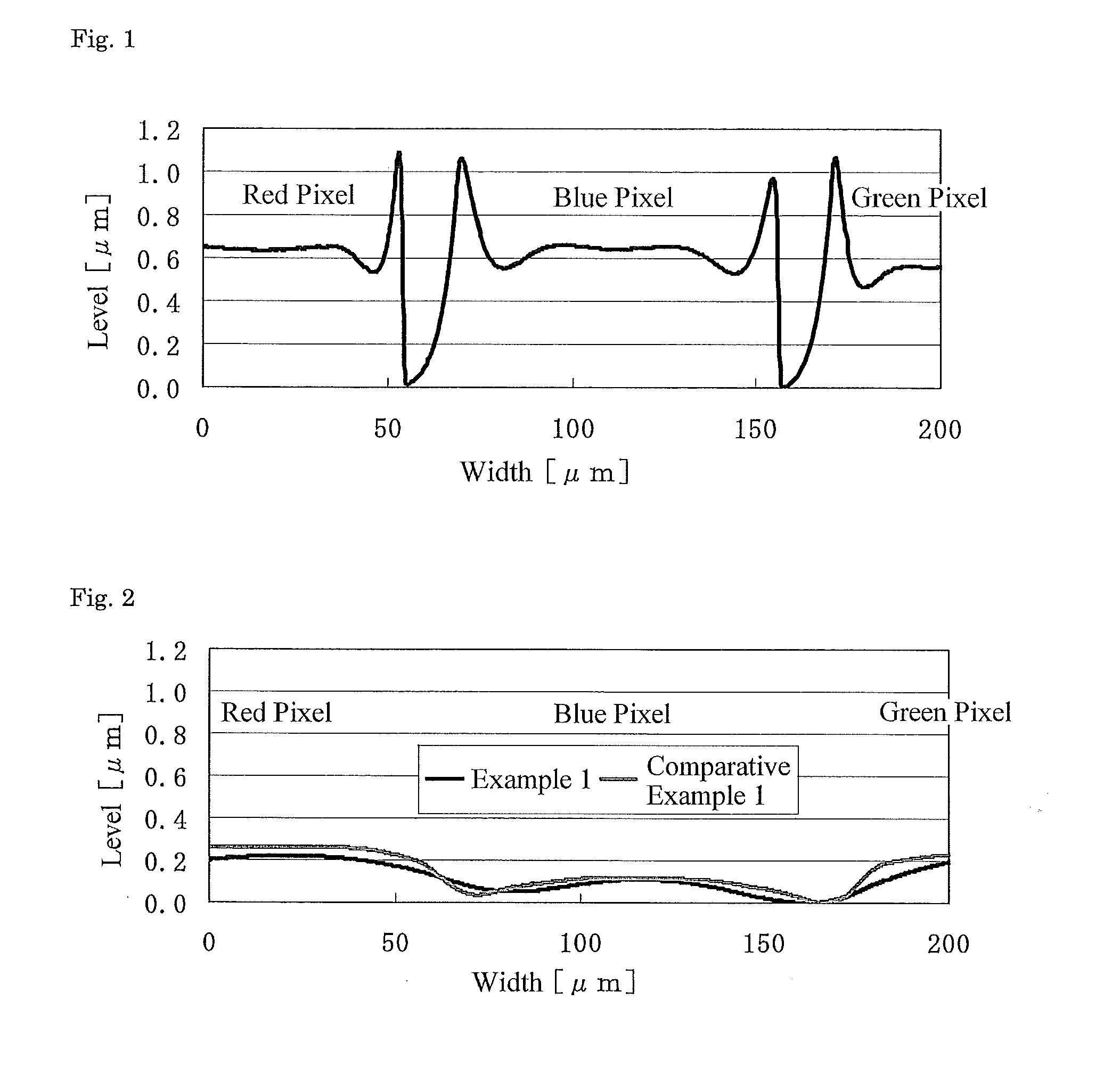
[0084]Coating liquid SM-1 for the smoothing layer was applied on the above color filter substrate, dried, and baked for one hour at 230° C. to prepare the substrate for liquid crystal display device of Example 1. The film thickness of the smoothing layer following baking was 6.3 μm.

example 2

[0087]The substrate for liquid crystal display device of Example 1 was subjected to a rubbing process. On the rubbed surface coating liquid LC-1 for optically anisotropic layer was applied, and the coating was dried for 2 minutes at a film surface temperature of 105° C. to obtain a liquid-crystal phase. The coating was then irradiated with UV radiation in air with a 160 W / cm air-cooled metal halide lamp (made by Eye Graphics Co., Ltd.) at a power density of 240 mW / cm2 and a dose of 600 mJ / cm2 to fix the orientation, yielding the substrate for liquid crystal display device of Example 2. The film thickness of the optically anisotropic layer was 1.2 μm.

example 3

[0090]The retardation of the smoothing layer was not measured on a color filter substrate, but instead using smoothing layer formed on a glass substrate by the same method as used in each example.

[0091]A non-alkali glass substrate was washed with a rotating brush having nylon bristles while spraying for 20 seconds a glass cleaning solution adjusted to 25° C., washed with a spray of pure water, and heated with a substrate preheating device for 2 minutes at 100° C. Subsequently, the substrate for retardation measurement of Example 3 was formed on this glass substrate by the same method as that used to form the smoothing layer in Example 1.


PUM

PropertyMeasurementUnit
Thicknessaaaaaaaaaa
Angleaaaaaaaaaa
Nanoscale particle sizeaaaaaaaaaa

Abstract

A substrate for liquid crystal display device comprising a layer having irregular differences in level and a smoothing layer provided directly on the layer having irregular differences in level, wherein the thickness of the smoothing layer is greater than the irregular differences in level, and the in-plane retardation of the layer inclined of 40° with the retardation axis as the axis of rotation is 5 to 150 nm, which enables to reduce the number of steps in manufacturing, is provided by the present invention.

Description

CROSS-REFERENCE TO RELATED APPLICATIONS[0001]This application claims benefit of priority under 35 USC 119 to Japanese Patent Application No. 2008-253392 filed on Sep. 30, 2008, the disclosure of which is expressly incorporated by reference herein in its entirety.TECHNICAL FIELD[0002]The present invention relates to a substrate for liquid crystal display device. More particularly, the present invention relates to a substrate for liquid crystal display device comprising, on an uneven layer, a smoothing layer functioning as an optically anisotropic layer, or functioning as an alignment layer and an optically anisotropic layer.BACKGROUND ART[0003]A CRT (cathode ray tube) has been mainly employed in various display devices used for office automation (OA) equipment such as a word processor, a notebook-sized personal computer and a personal computer monitor, mobile phone terminal and television set. In recent years, a liquid crystal display device has more widely been used in place of a CR...

Claims


Application Information

Patent Timeline
IPC IPC(8): G02F1/1347G02F1/13363C08G73/10
CPCC08G73/101C08G73/1042C08G73/1075G02F2001/133357C08G73/12C08L79/08C08L79/085C08G73/1078G02F1/133357
Inventor NAKAJIMA, MASAOIMAKUNI, AKIRA
Owner FUJIFILM CORP
Why Eureka
Try Eureka