Method of manufacturing a semiconductor device

a manufacturing method and semiconductor technology, applied in the direction of individual semiconductor device testing, semiconductor/solid-state device testing/measurement, instruments, etc., can solve the problems of reducing production yield, difficult to completely control all diffusion parameters that affect the electrical characteristics at a target value, and inability to inspect all processed wafers in the semiconductor manufacturing apparatus from a cost perspective, etc., to achieve high accuracy and high accuracy

Inactive Publication Date: 2010-04-01
PANASONIC CORP
View PDF7 Cites 4 Cited by
  • Summary
  • Abstract
  • Description
  • Claims
  • Application Information

AI Technical Summary

Benefits of technology

[0009]The present invention has been proposed by taking such problem into consideration, and has the objective of providing a method of manufacturing a semiconductor device where electrical characteristics are predicted with high accuracy, and the electrical characteristics are controlled to become constant using the prediction expression.
[0010]In order to accomplish this objective, the present invention has adopted the following means. The present invention realizes uniformity of electrical characteristics of semiconductor devices to be formed on different wafers using an electrical characteristic prediction expression showing an electrical characteristic with diffusion parameters reflecting a post-processing configuration, such as a film thickness to be deposited on a semiconductor substrate, finished dimensions of fabricated patterns, or the like. Conventionally, it is a newly-discovered finding by the inventors of the present application that results of electrical measurement implemented at a time of completing entire processes or at a time of completing a specific process can be predicted with high accuracy by the electrical characteristic prediction expression.

Problems solved by technology

However, it is not realistic to inspect all processed wafers in the semiconductor manufacturing apparatus from a cost standpoint.
Therefore, even if the APC is implemented, it would be difficult to completely control all of the diffusion parameters that affect the electrical characteristics at a target value.
As a result, the electrical characteristics of the semiconductor device vary according to the variation of the diffusion parameters and production yield is decreased.
Further, since the prediction expression is a statistical model and it is not generalized, the prediction accuracy is not always guaranteed.
Therefore, it is difficult to control the electrical characteristics according to the prediction expression.

Method used


Image

  • Method of manufacturing a semiconductor device
  • Method of manufacturing a semiconductor device
  • Method of manufacturing a semiconductor device

Examples


first embodiment

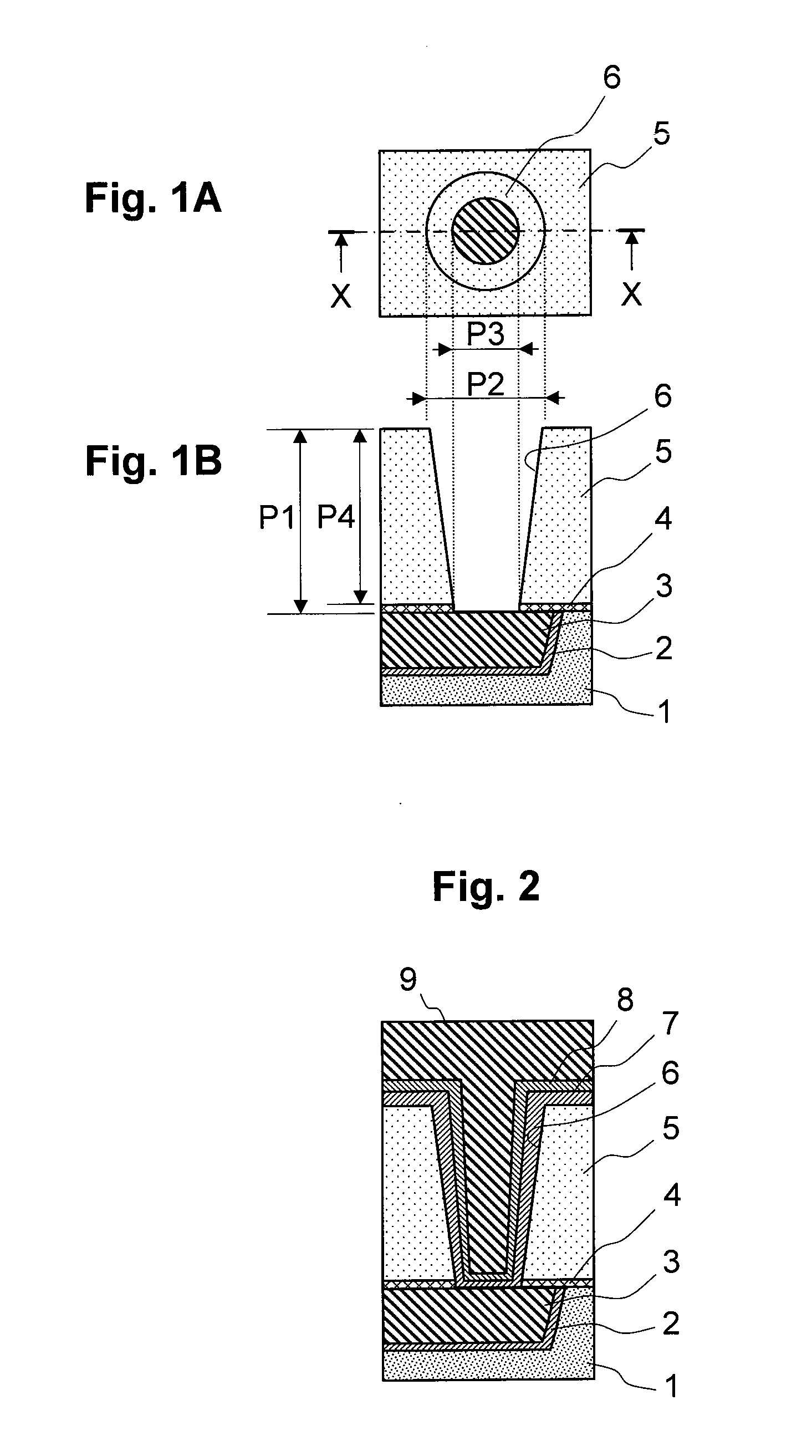
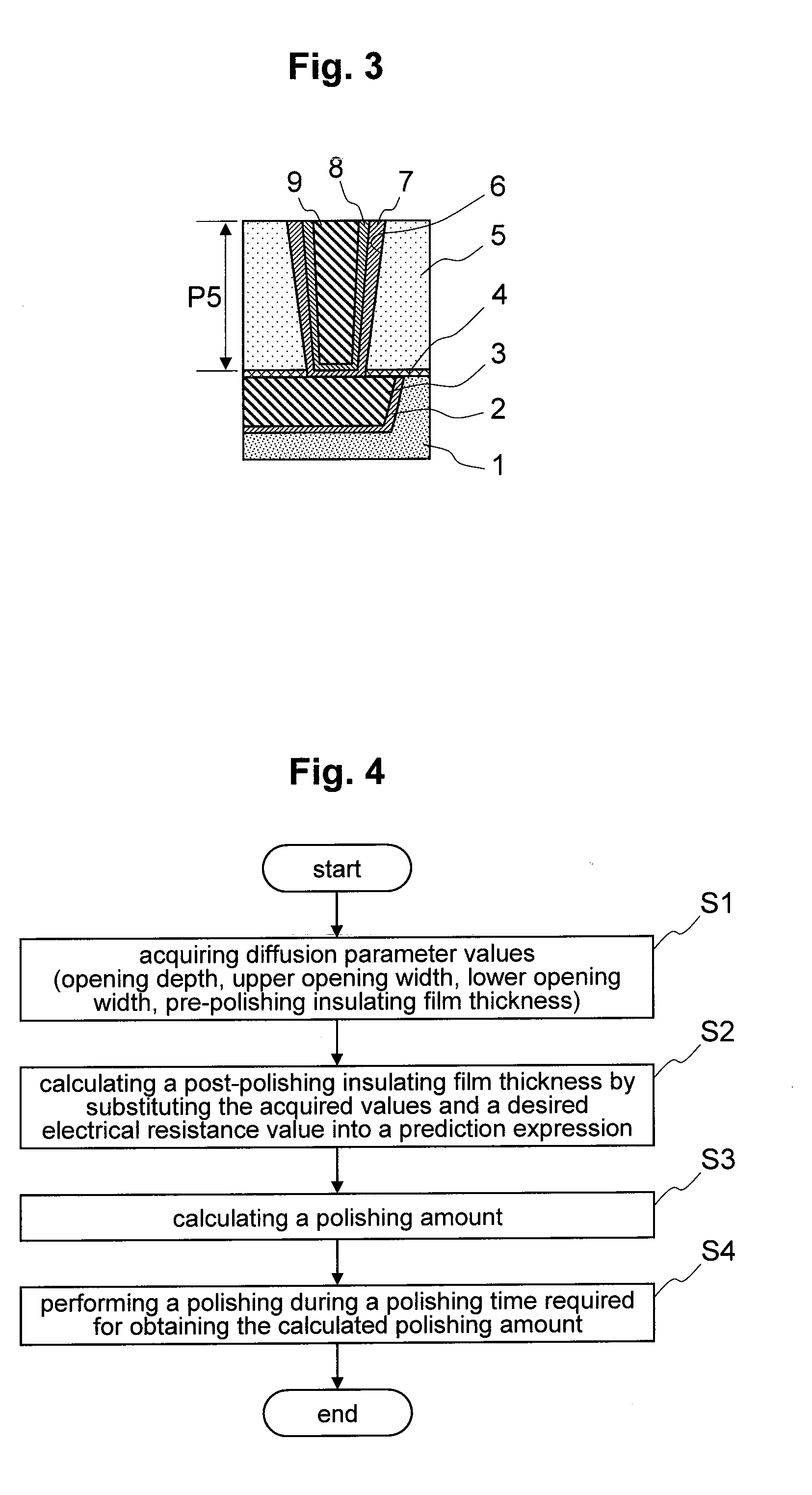
[0037]In a first embodiment, a method for determining a processing condition (fabricating condition) using an electrical characteristic prediction expression of a semiconductor device. Prior to the explanation, first, an example of a structure of a semiconductor device where the prediction expression is applied is briefly explained along with a manufacturing process thereof. FIGS. 1A to 3 are diagrams showing a formation process of a wiring in a semiconductor device having an embedded wiring. Furthermore, FIG. 1A is an enlarged plane view showing a periphery of a concave portion where the wiring is embedded, and FIG. 1B is a cross sectional view along the X-X line shown in FIG. 1A. Further, FIGS. 2 and 3 show only cross sectional views corresponding to the X-X line of FIG. 1A.

[0038]First, as shown in FIGS. 1A and 1B, a first interlayer insulating film layer 1 made of a silicon oxide film and the like is deposited on a semiconductor substrate (not illustrated) where a semiconductor e...

second embodiment

[0063]In a second embodiment, in addition to the technique to unify the electrical characteristics explained in the first embodiment, a technique to predict results of electrical characteristic examination (WET: Wafer Electric Test or PCM measurement) to be implemented at a time of completing an entire processes for the wafer or at a time of completing a specific process by using the unification technique and to recover a wafer to be defective in the electrical characteristic examination is explained. In other words, in this embodiment, in a semiconductor manufacturing apparatus that can actually adjust a value of a specific parameter by changing processing conditions, the processing is implemented under processing conditions where the diffusion parameter is equal to the predicted value and the electrical characteristic after the processing is predicted according to the electrical characteristic prediction expression. Then, whether the electrical characteristic will be defect on the...

third embodiment

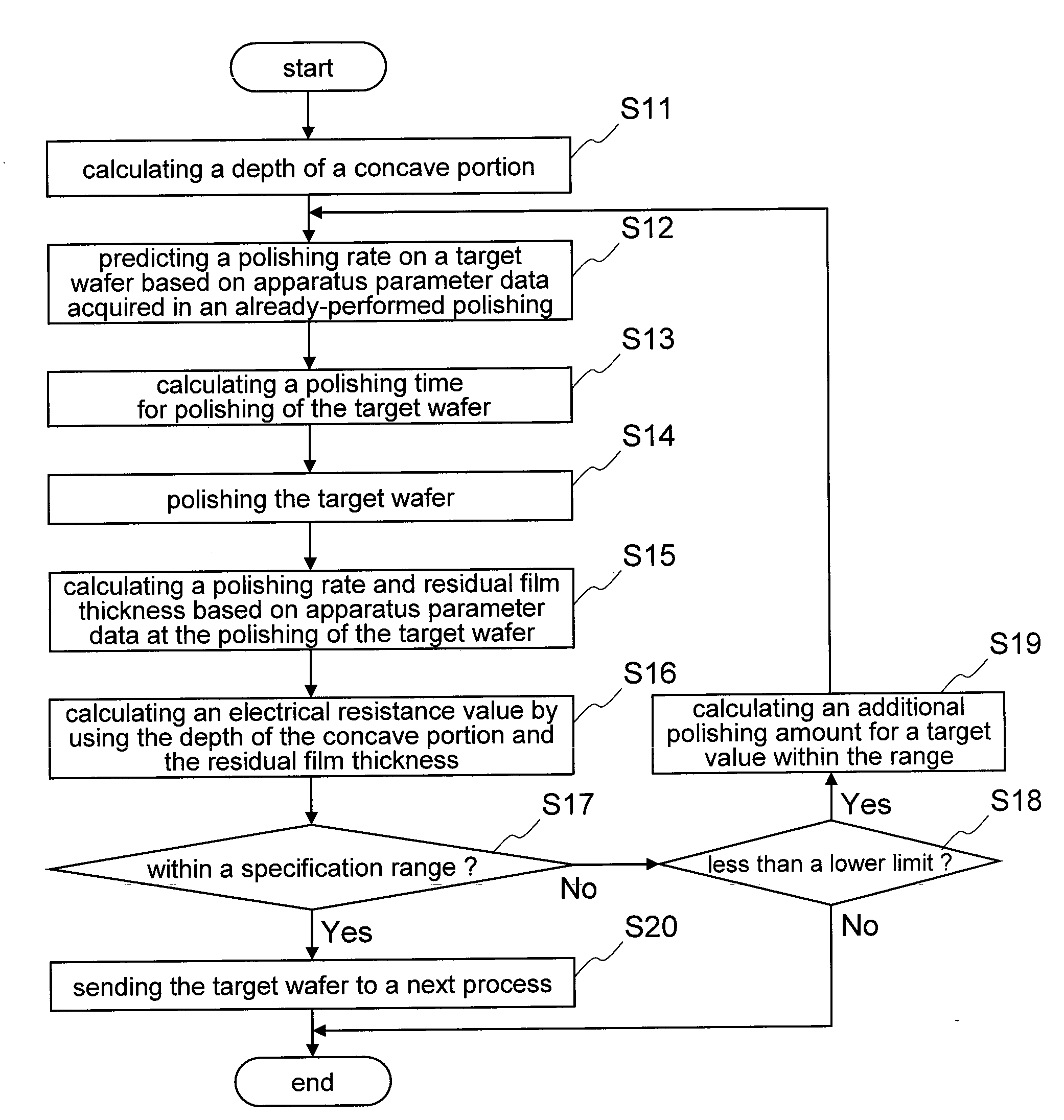
[0080]In the second embodiment, since the electrical resistance value is predicted after polishing is implemented and the determination is conducted based upon the predicted electrical resistance value, wafers whose electrical resistance value is beyond the specification range and is high resistance cannot be recovered. Then, in a third embodiment, a configuration to enable a prevention of occurrence of such wafer is explained.

[0081]FIG. 8 is a configuration diagram showing a semiconductor manufacturing system to realize a method of manufacturing a semiconductor device in this embodiment. As shown in FIG. 8, although an APC system 80 of this semiconductor manufacturing system has the same components as those in the APC system 60 described in the second embodiment, a data transmission path and a transmission order are different as described below. According to this configuration, the APC system 80 in this embodiment predicts the electrical resistance value of a target wafer before po...


PUM


Abstract

In the method of manufacturing a semiconductor device, first, values of diffusion parameters of a semiconductor device are acquired in a middle of manufacturing the semiconductor device. Next, a target value of another diffusion parameter to be determined by a processing implemented in a subsequent process of the semiconductor device manufacturing process is calculated. The another diffusion parameter is calculated by substituting the acquired values of diffusion parameters and a desired value of an electrical characteristic of the semiconductor device into a predetermined prediction expression. The prediction expression is an expression showing a corresponding relationship between the electrical characteristic and a plurality of types of diffusion parameters of the semiconductor device. Subsequently, processing conditions for the processing implemented in the subsequent process to realize the target value is determined. Then, the processing to the semiconductor device in the subsequent process is implemented under the determined processing conditions.

Description

CROSS-REFERENCE TO RELATED APPLICATION[0001]The disclosure of Japanese Patent Application No. 2008-254657 filed Sep. 30, 2008 including specification, drawings and claims is incorporated herein by reference in its entirety.BACKGROUND OF THE INVENTION[0002]1. Field of the Invention[0003]The present invention relates to a method of manufacturing a semiconductor device, and particularly relates to a method of manufacturing a semiconductor device where electrical characteristics of semiconductor devices to be formed on different wafers can be made uniform.[0004]2. Description of the Related Art[0005]In a manufacturing process of semiconductor devices, various apparatuses, such as an exposure apparatus, an implantation apparatus, a thermal treatment apparatus, a film-forming apparatus, an etching apparatus or a polishing apparatus (hereafter, referred to as semiconductor manufacturing apparatus), are used. Processing variations caused by fluctuation of an apparatus condition of such semi...

Claims


Application Information

Patent Timeline
Patent Type & Authority Applications(United States)
IPC IPC(8): H01L21/66
CPCH01L22/12H01L22/20H01L2924/0002H01L2924/00
Inventor TANAKA, TOMOYAIMAI, SHIN-ICHI
Owner PANASONIC CORP
Why Eureka
Try Eureka