Lead-Free Solder with Improved Properties at Temperatures >150°C

a technology of lead-free solder and improved properties, applied in the field of solder, can solve the problem that indium alloys are not suitable for the production of solder balls for chip fabrication

Inactive Publication Date: 2010-04-08
HERAEUS MATERIALS TECHNOLOGY GMBH & CO KG
View PDF5 Cites 34 Cited by
  • Summary
  • Abstract
  • Description
  • Claims
  • Application Information

AI Technical Summary

Benefits of technology

[0010]The object of the present invention lies in counteracting the material fatigue that occurs at temperatures up to 200° C., particularly in the range between 150 and 190° C.
[0028]According to a further embodiment of the invention, on one hand, the formation of metallic phases is kept small and, on the other hand, the crystallization of the intermetallic phases is modified. Higher copper or silver portions increase the formation of intermetallic phases. Here, it is significant that, between 1 and 8 wt. % indium, particularly between 1.5 and 5 wt. % indium, the formation of a Cu3Sn phase for the application of the solder on a Cu surface is significantly restricted. It is further significant that the crystallization growth is modified. Both effects slow material fatigue at high temperatures; in particular, so far as the silver content is limited to a maximum of 3.5 wt. %, in particular 3 wt. %.
[0035]Also very important is the dosing of indium. Indium appears to decisively block the growth of the Cu3Sn phase. For this purpose, between 1 to 2 wt. % indium is required in order to block the formation of Cu3Sn phase significantly. With 1% indium and just below, the phase growth of the Cu3Sn phase is similar to that of a pure SAC solder (Sn, Ag, Cu). At 1.75 wt. %, a significantly smaller phase growth of the Cu3Sn phase has been found, and associated with this a longer high-temperature stability. Indium is the most expensive of all the components and is already used as sparingly as possible for this reason. Thus, the expensive cost effect in the range between 5 to 8 wt. % indium is relatively small. Above 8% indium, the melting point of the solder is too low for the high-temperature applications intended for the solders according to the invention. The tensile strength increases as a function of the indium content, whereby for this aspect, an indium content between 4 and 10 wt. %, particularly between 4 and 8 wt. %, can be justified.
[0044]The solders according to the invention allow more reliable electronics at application temperatures of the electronics in the range between 140 and 200° C., particularly between 150 and 190° C. or under high temperature-change conditions. The solders according to the invention increase the reliability of the power electronics and the high-temperature applications, particularly power electronics in high-temperature applications. As examples for the power electronics the following can be named: DCB (direct copper bonding), COB (chip on board), hybrid circuits, semiconductors, wafer bumping, SIP (system in packaging), and MCM (multi chip module), particularly stack package. The risk of electrical short circuits due to growth of Ag3Sn phases in closely spaced solder connections, as in wafer bumping, is considerably reduced with solders according to the invention.
[0045]The temperature range between 140 to 200° C., particularly 150 to 190° C., is of considerable importance for electronic solder connections in machine construction, particularly vehicle construction, whereby increased security is ensured for electronics with solders according to the invention in machine and vehicle construction. Particularly in this field, in addition to temperature loads, the temperature-change stability is also important and improved with the solders according to the invention. The improved security with the solders according to the invention in the high temperature range is particularly important for the automotive, industrial electronics, rail vehicles, and aerospace fields. Especially, the electronics in the fields of motors, driving mechanisms, or brakes are already exposed to extreme temperature loading and should nevertheless exhibit maximum reliability, whereby in the case of power electronics, the heat generated by the electronics still negatively affects the reliability. The solders according to the invention will significantly contribute to alleviating problems in these technical fields. Furthermore, the solders according to the invention aid the reliability for increased security in electronics exposed to solar radiation, particularly electronics exposed to direct solar radiation, but also electronics impacted by indirect solar radiation.

Problems solved by technology

The high indium content makes the solder alloys very soft, and deformations (holes) appear, so that these indium alloys are not suitable for the production of solder balls for chip fabrication.

Method used


Image

  • Lead-Free Solder with Improved Properties at Temperatures >150°C
  • Lead-Free Solder with Improved Properties at Temperatures >150°C
  • Lead-Free Solder with Improved Properties at Temperatures >150°C

Examples


invention example 1

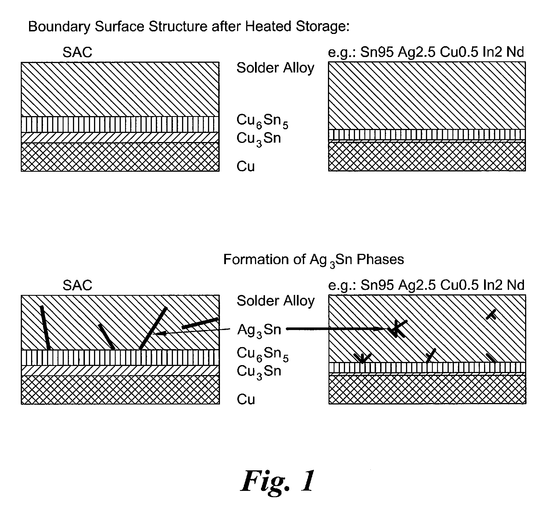
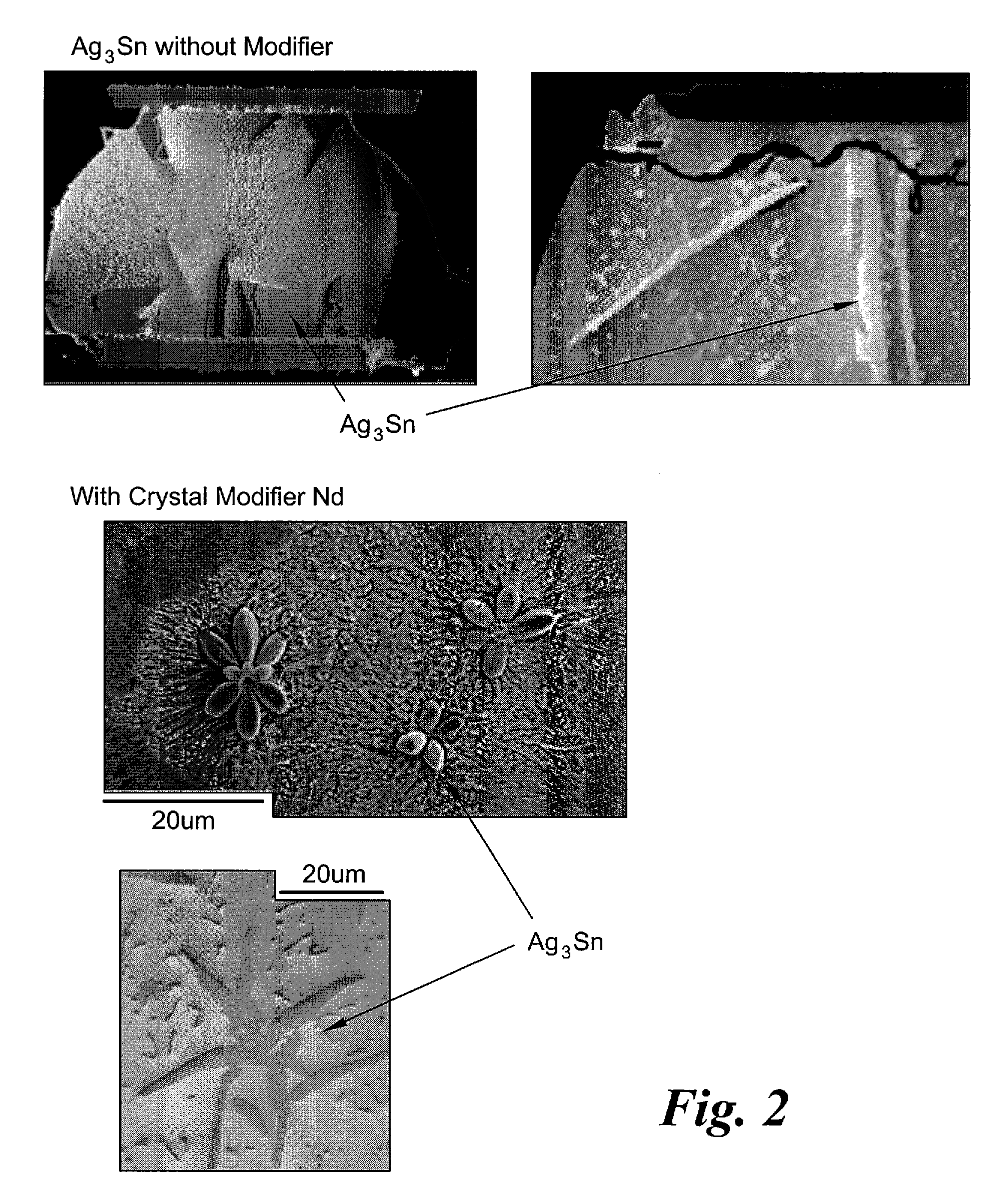
[0069]Sn 95.49, Ag 2, Cu 0.5, In 2, Nd 0.01 shows, in addition to further improved mechanical properties compared with Comparison Example 4, a suppressed formation of the Cu3Sn phase and a lower growth of the same at temperatures above 150° C. With this example according to the invention, the material fatigue is drastically slowed down thereby with excellent mechanical properties.

[0070]If the doping with neodymium from Example 1 is discontinued according to Comparison Example 5, the formation of the Cu3Sn phase is indeed small at the beginning, but the Ag3Sn phase tends toward growth and the formation of coarse plates or needles at temperatures above 150° C. and therefore leads to unacceptable material fatigue and the risk of short circuit formation due to the crystal growth of Ag3Sn.

invention example 2

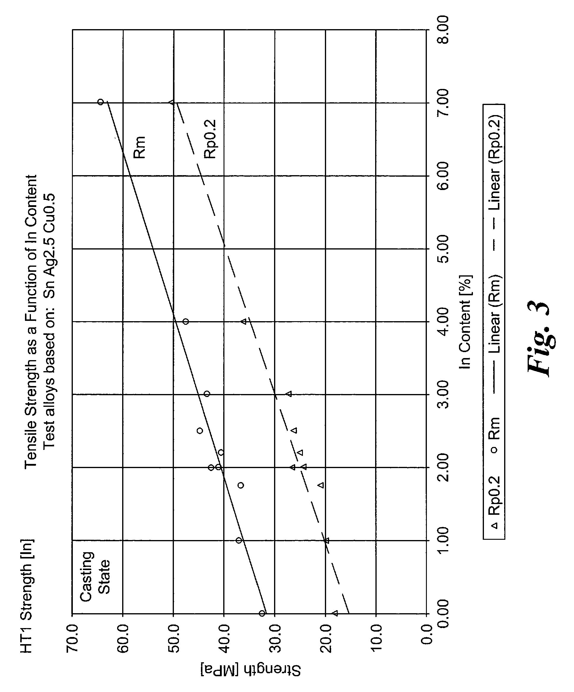
[0071]Example 2 with an increase in the indium concentration by 1%, compared with Example 1, causes further improved mechanical properties. The formation of the Cu3Sn phase when soldered on a copper track is further reduced, compared with Example 1, and the material fatigue diminishes even more at temperatures above 150° C.

invention example 3

[0072]A further increase of 1 wt. % indium according to Example 3 produces, in addition to more improved mechanical properties, no relevant decrease in the formation of the Cu3Sn phase compared with Example 2. The material fatigue at temperatures above 150° C. is reduced compared with Example 2.


PUM

PropertyMeasurementUnit
melting temperatureaaaaaaaaaa
temperaturesaaaaaaaaaa

Abstract

Lead-free solders based on an Sn—In—Ag solder alloy contain 88 to 98.5 wt. % Sn, 1 to 10 wt. % In, 0.5 to 3.5 wt. % Ag, 0 to 1 wt. % Cu, and a doping with a crystallization modifier, the crystallization modifier preferably being a maximum of 100 ppm neodymium.

Description

CROSS-REFERENCE TO RELATED APPLICATIONS[0001]This application is a Section 371 of International Application No. PCT / EP2007 / 008635, filed Oct. 5, 2007, which was published in the German language on Apr. 17, 2008, under International Publication No. WO 2008 / 043482 A1 and the disclosure of which is incorporated herein by reference.BACKGROUND OF THE INVENTION[0002]The present invention relates to a solder for objects whose use range lies up to 200° C., in particular 150 to 190° C.[0003]At these high temperatures, tin-silver-copper (SAC) solder points age particularly quickly due to the growth of intermetallic phases. The tensile strength is lower at high temperatures and the permanent elongation limit worsens due to the material fatigue, which follows in association with the growth of the intermetallic phases.[0004]According to EU guidelines 2002 / 96 / EG “Waste Electrical and Electronic Equipment” (WEEE) and 2002 / 95 / EG “Restriction of the use of certain hazardous substances in electrical ...

Claims


Application Information

Patent Timeline
Patent Type & Authority Applications(United States)
IPC IPC(8): B23K35/26B23K35/24
CPCB23K35/262H01L2924/3651C22C13/00B23K1/0016B23K35/22B23K35/24B23K2101/36
Inventor KRAEMER, WINFRIEDTRODLER, JOERG
Owner HERAEUS MATERIALS TECHNOLOGY GMBH & CO KG
Why Eureka
Try Eureka