
Method for forming dual damascene structure

a damascene and structure technology, applied in the direction of instruments, semiconductor/solid-state device testing/measurement, measurement devices, etc., can solve the problems of copper wires not being patterned by the conventional methods used to pattern al wires, copper failure to form highly volatile chlorides, and less and less qualified aluminum for interconnection of elements

Active Publication Date: 2010-04-08
UNITED MICROELECTRONICS CORP
View PDF5 Cites 0 Cited by
  • Summary
  • Abstract
  • Description
  • Claims
  • Application Information

AI Technical Summary

Benefits of technology

[0016]In the method for forming a dual damascene structure and for determining the thickness of a photo resist layer of the present invention, a periodic parameter is taken into consideration so that a correct etching depth can be reached and all the materials of the interlayer dielectric layer in the vias can be thoroughly removed by etching during the etching of the interlayer dielectric layer. An effective metal interconnect structure is hence formed to ensure good electric connections between the elements in the semiconductor.

Problems solved by technology

However, with the shrinkage of the element critical dimension (CD) and the obvious behavior of electromigration, aluminum is less and less qualified to be used for the formation of interconnect of elements.
However, there are severe problems coming with the usage of copper to replace aluminum for the formation of interconnect of elements, which are highly incompatible with the conventional Al process, i.e. the copper wires cannot be patterned by the conventional methods used to pattern the Al wires.
On one hand, copper fails to form highly volatile chlorides so the dry etching techniques used in the conventional Al process cannot be applied in the copper process.
On the other hand, because the wet etching of copper suffers severe under-cut, the narrower the line width the severer the problem, the only practical method available on the production line is the damascene process.

Method used


Image

  • Method for forming dual damascene structure
  • Method for forming dual damascene structure
  • Method for forming dual damascene structure

Examples


Embodiment Construction

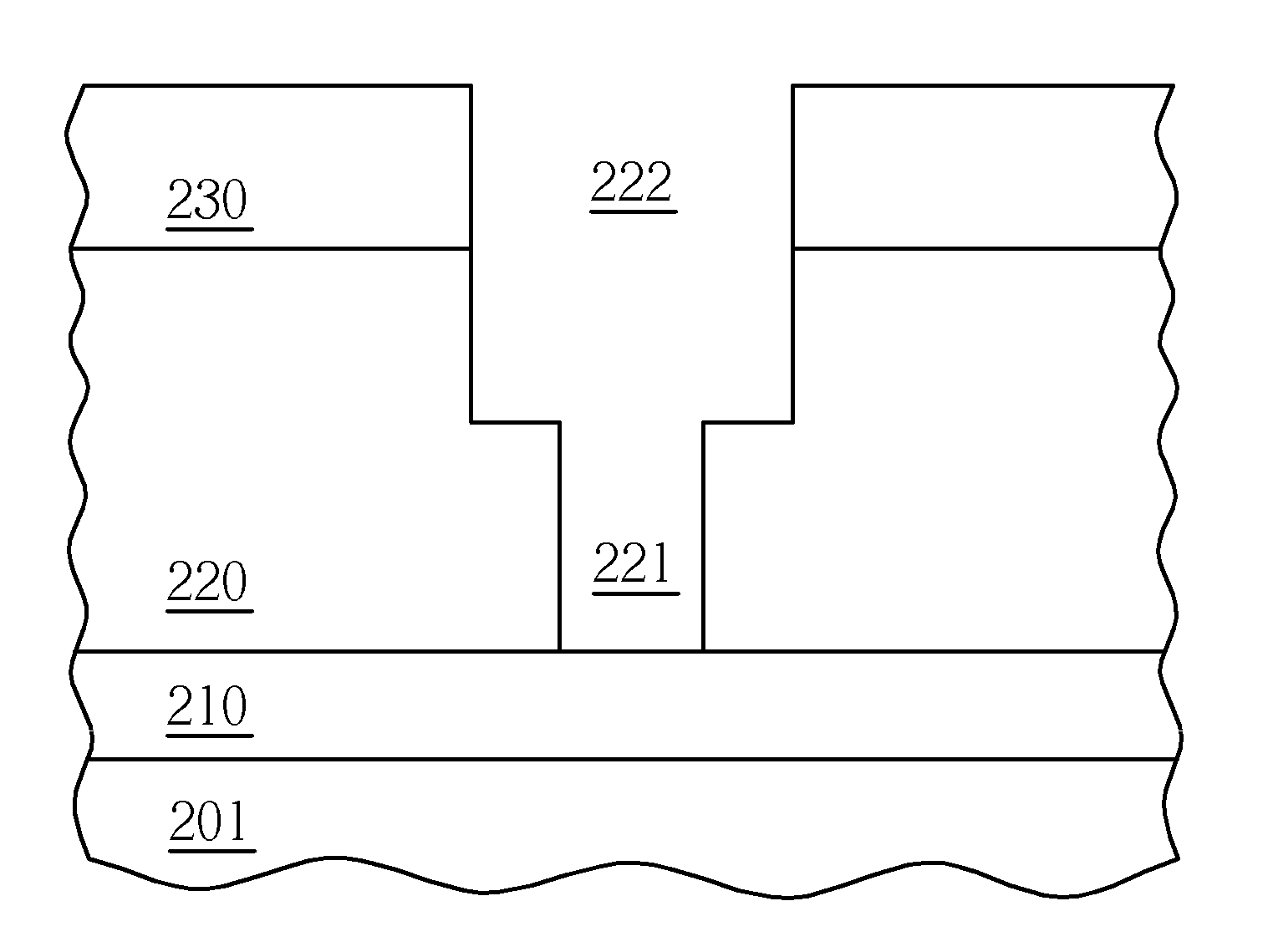
[0020]The present invention proposes a method for forming a dual damascene structure and for determining the thickness of a photo resist layer. In the method for forming a dual damascene structure and for determining the thickness of a photo resist layer of the present invention, because a periodic parameter derived from the exposure light source is taken into consideration, it facilitates the estimation of the correct thickness of the photo resist layer. As a result, a correct etching depth can be reached and all the materials of the interlayer dielectric layer and the photo resist layer in the vias can be thoroughly removed by lithography and etching during the following etching procedure of the interlayer dielectric layer. An effective metal interconnect structure is hence formed to ensure good electric connections between the elements in the semiconductor.

[0021]The present invention first provides a method for forming a dual damascene structure. FIGS. 6-11 illustrate a preferred...


PUM


Abstract

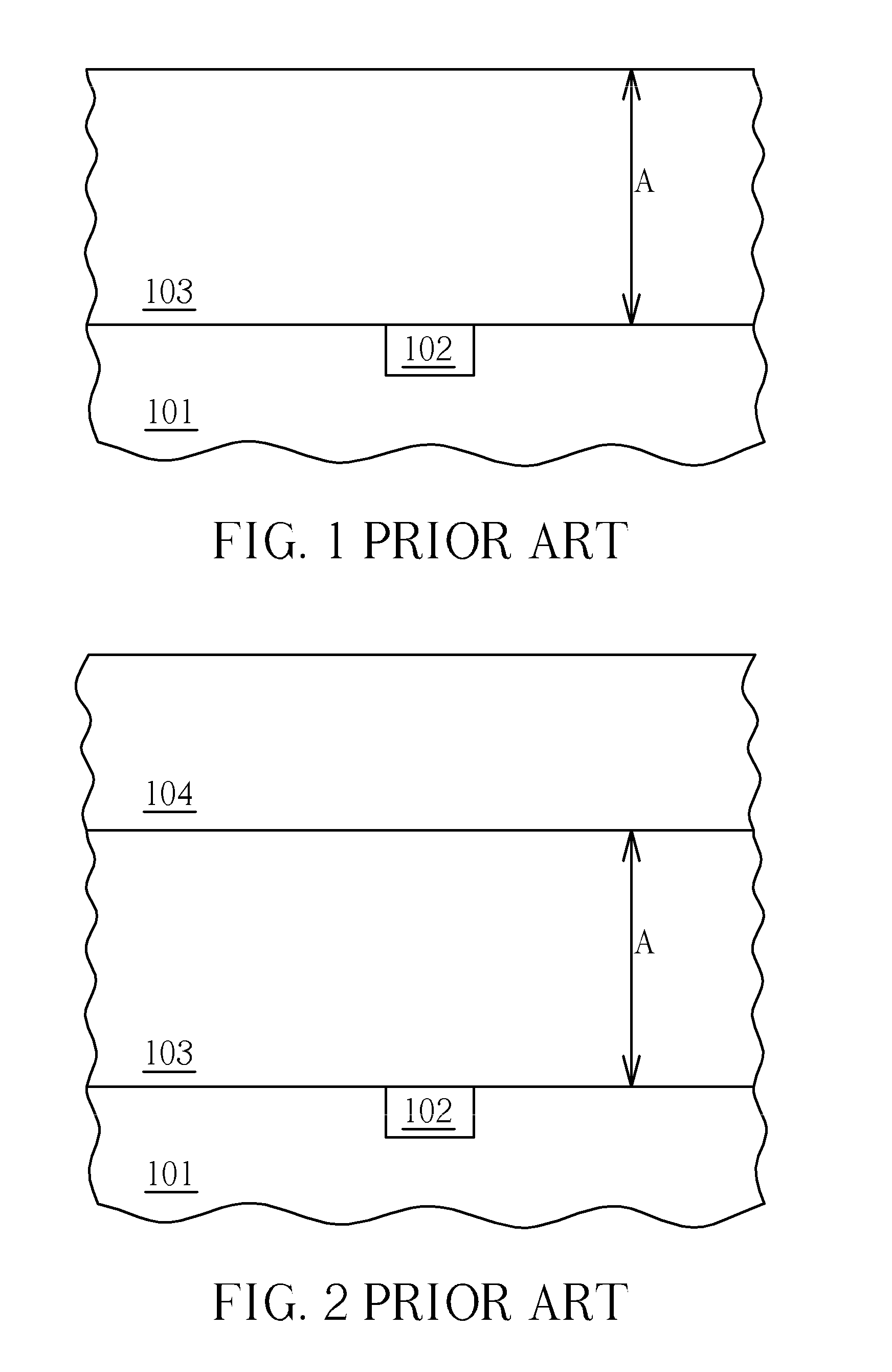
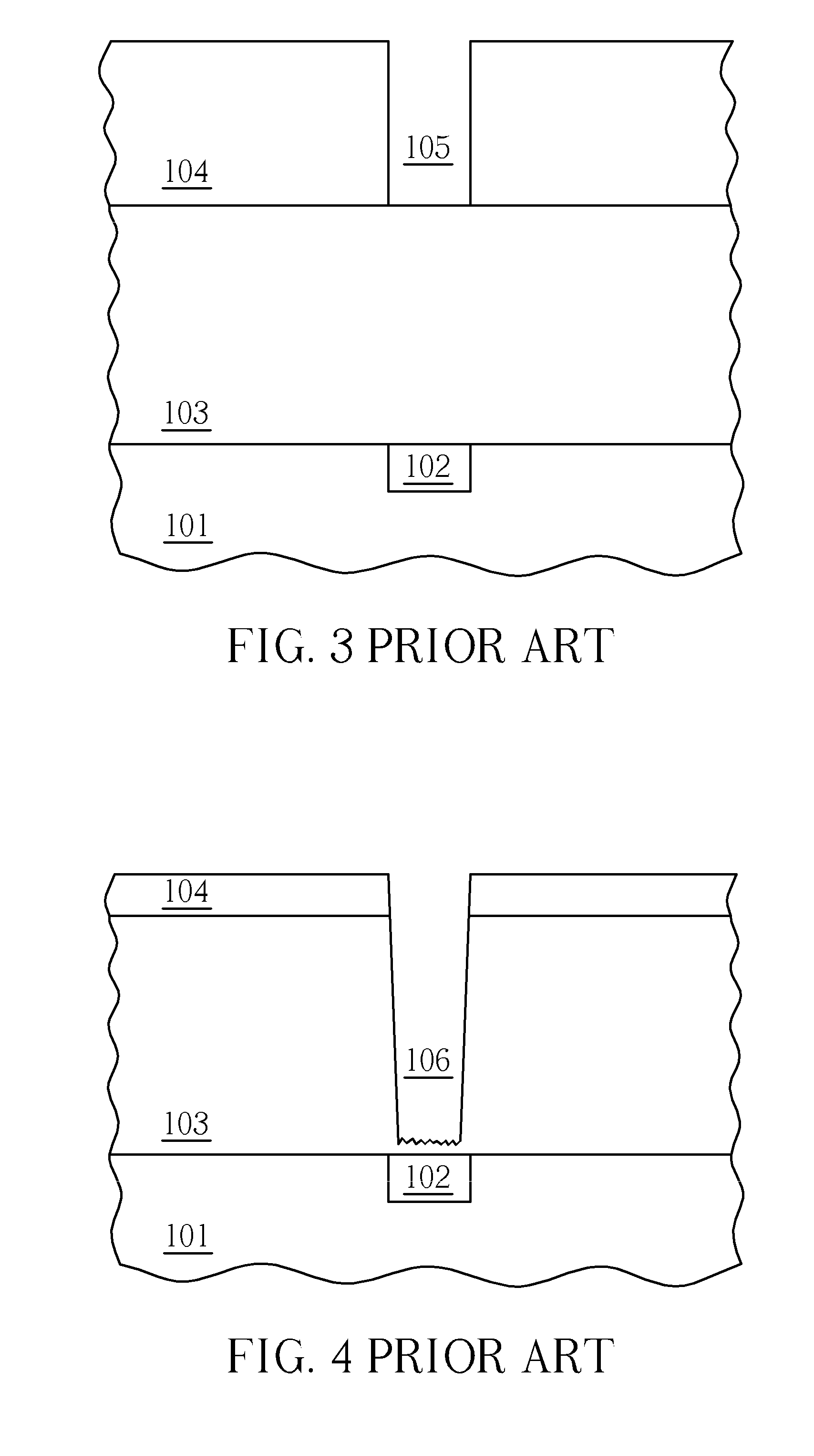
A method for forming a dual damascene structure is disclosed. First a substrate is provided. There are an etching stop layer and an interlayer dielectric layer disposed on the substrate in order. The interlayer dielectric layer has a thickness A. Second, the interlayer dielectric layer is patterned to form a first opening. Later, a photo resist layer with a thickness B is formed on the interlayer dielectric layer. Then, the photo resist layer is patterned by a light source to construct a patterned photo resist layer. Later, the interlayer dielectric layer is again patterned by the patterned photo resist to pattern the interlayer dielectric layer to construct a second opening on the first opening by means of a light source and the photo resist layer so as to form a dual damascene structure. The light source has a periodic parameter C so that (A+B) / C≈X / 2, where X is an odd number.

Description

BACKGROUND OF THE INVENTION[0001]1. Field of the Invention[0002]The present invention relates to a method for forming a dual damascene structure. In particular, the present invention relates to a method for forming a dual damascene structure by calculating a periodic parameter.[0003]2. Description of the Prior Art[0004]In the manufacturing process of semiconductors, metals are used for the formation of interconnect of elements. Aluminum used to be used for the formation of interconnect of elements. However, with the shrinkage of the element critical dimension (CD) and the obvious behavior of electromigration, aluminum is less and less qualified to be used for the formation of interconnect of elements. Currently, copper is generally used to replace aluminum for the formation of interconnect of elements because copper has a much lower electric resistance, better RC delay time and weaker behavior of electromigration.[0005]In addition to the much lower electric resistance, the reasons w...

Claims


Application Information

Patent Timeline
Patent Type & Authority Applications(United States)
IPC IPC(8): H01L21/66
CPCH01L21/76813H01L21/76807
Inventor XIE, YONG-GANG
Owner UNITED MICROELECTRONICS CORP
Learn More