Circuit for clearing CMOS information

Inactive Publication Date: 2010-04-15
HONG FU JIN PRECISION IND (SHENZHEN) CO LTD +1
View PDF1 Cites 14 Cited by
  • Summary
  • Abstract
  • Description
  • Claims
  • Application Information

AI Technical Summary

Problems solved by technology

However, using the jumper to clear the CMOS information is time-consuming and inefficient because t

Method used


Image

  • Circuit for clearing CMOS information
  • Circuit for clearing CMOS information
  • Circuit for clearing CMOS information

Examples


Embodiment Construction

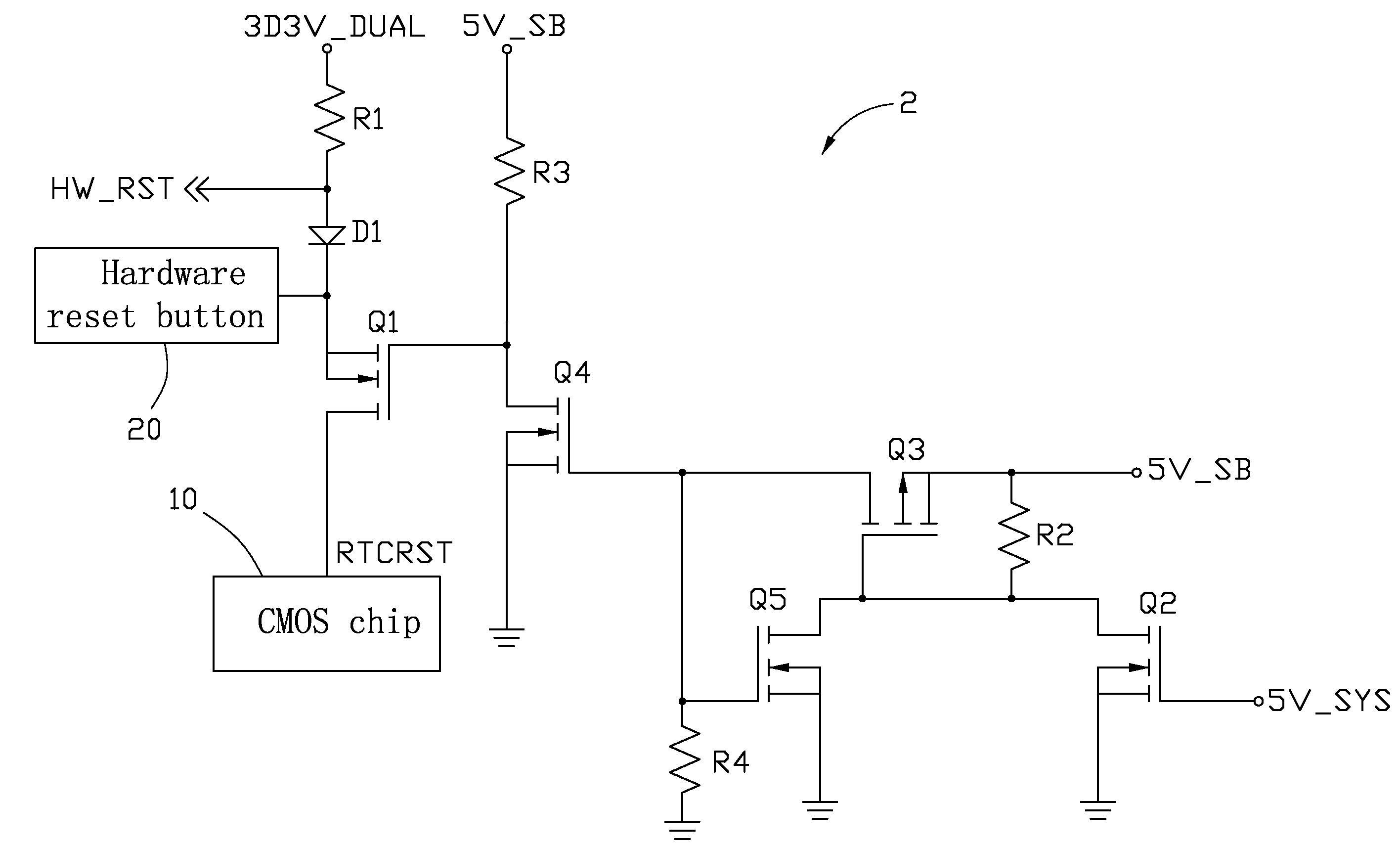
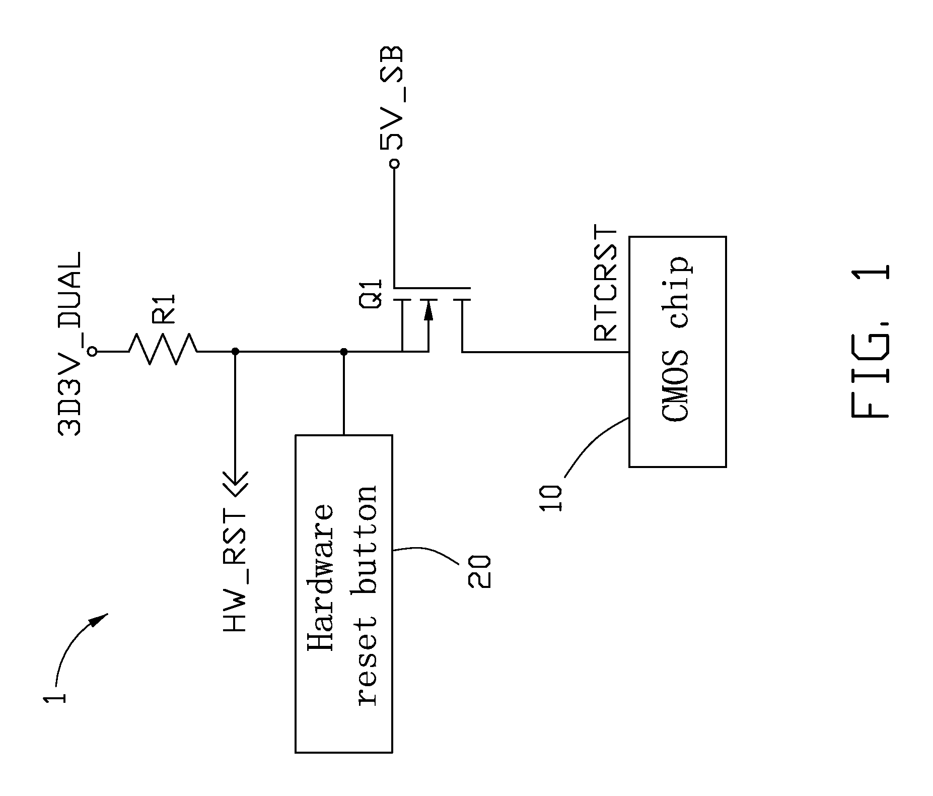
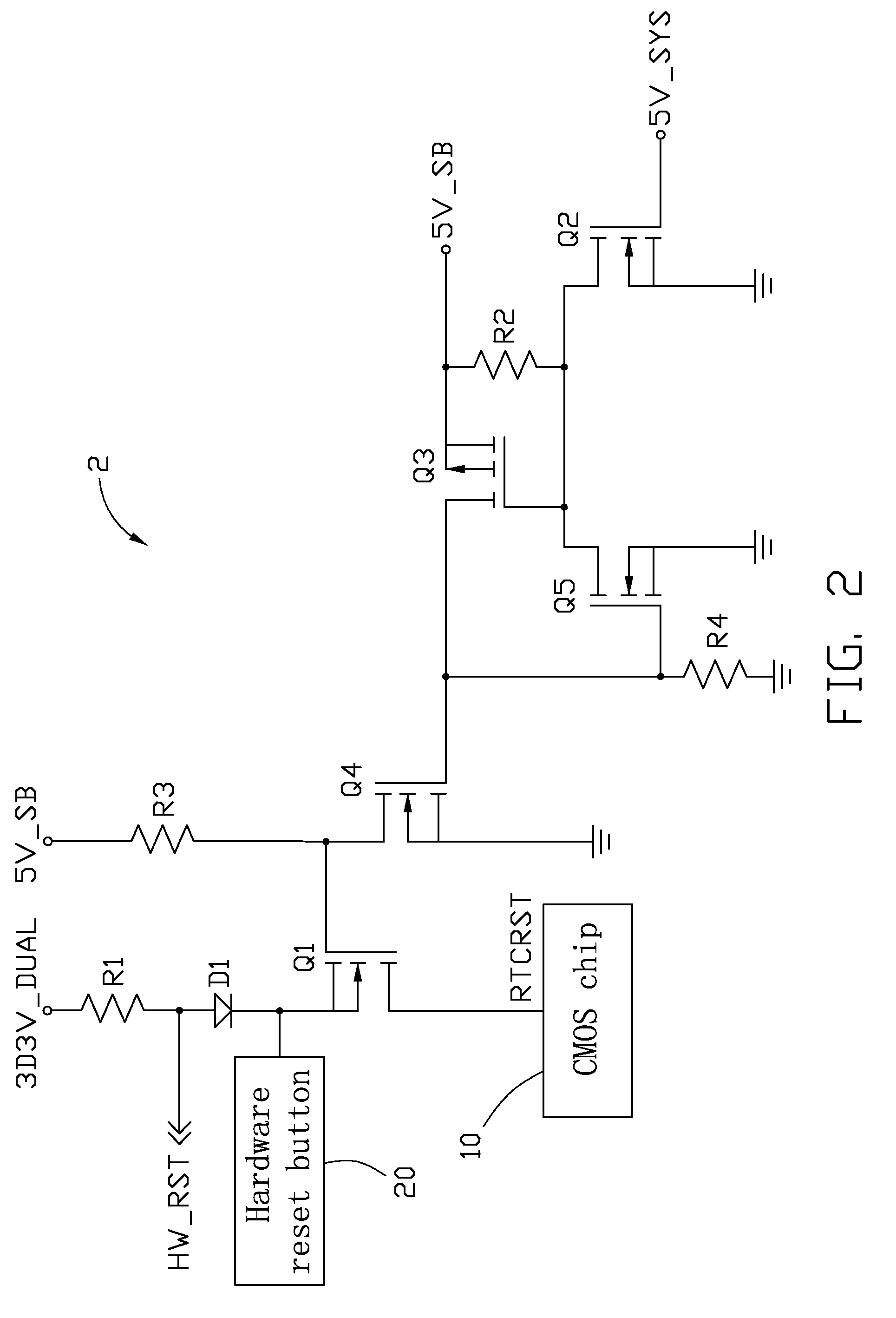
[0009]Referring to FIG. 1, a circuit 1 for clearing CMOS information of a CMOS chip 10 of a computer includes an electronic switch Q1 and a resistor R1. In the illustrated embodiment of FIG. 1, the electronic switch Q1 is an N-channel metal oxide semiconductor field effect transistor (MOSFET), which includes a gate, a drain, and a source. In other embodiments, the electronic switch Q1 may be a negative-positive-negative (NPN) bipolar junction transistor (BJT), which includes a base, a collector, and an emitter.

[0010]The gate of the transistor Q1 is connected to a standby power supply 5V_SB which may supply 5V of power to the transistor Q1 in one particular embodiment. The drain of the transistor Q1 is connected to a software reset pin, such as a real time clock reset (RTCRST) pin of a CMOS chip 10. The source of the transistor Q1 is connected to a hardware reset (HW_RST) pin of the computer, and is also connected to a dual power supply 3D3V_DUAL of the computer via the resistor R1. ...


PUM


Abstract

A circuit for clearing complementary metal oxide semiconductor (CMOS) information of a CMOS chip of a computer includes a resistor and an electronic switch. The electronic switch includes a first terminal, a second terminal, and a third terminal. The first terminal is connected to a standby power supply of the computer. The second terminal is connected to a software reset pin of the CMOS chip. The third terminal is connected to a dual power supply of the computer via the resistor, and is connected to a hardware reset pin of the computer. The standby power supply is provided, and the first electronic switch is turned on before the computer is booted up. The software reset pin may be triggered to clear CMOS information of the CMOS chip upon the condition that the hardware reset pin is triggered.

Description

BACKGROUND[0001]1. Technical Field[0002]The present disclosure relates to computer circuits, and particularly to a circuit for clearing complementary metal oxide semiconductor (CMOS) information of a computer.[0003]2. Description of the Related Art[0004]With regards to electronics, and particularly to computer electronics, jumpers are generally used to adjust connections of electrical components on printed circuit boards, such as motherboards of computers. Jumper pins (points to be connected by the jumper) are arranged in groups called jumper blocks, with each group having at least one pair of contact points and often more. In general, each contact point in a jumper block terminates using a small metal pin. An appropriately sized conductive sleeve called a jumper, or more technically, a jumper shunt, is slipped over the pins to complete the circuit.[0005]Jumper blocks and jumpers are often used on a motherboard to maintain power supply to a south bridge chip thus safeguarding comple...

Claims


Application Information

Patent Timeline
IPC IPC(8): H03L7/00
CPCG11C7/20G06F1/24
Inventor SHI, LEI
Owner HONG FU JIN PRECISION IND (SHENZHEN) CO LTD
Why Eureka
Try Eureka