High Temperature Solder Materials

a technology of soldering materials and high temperature, applied in the direction of soldering equipment, metal-working equipment, manufacturing tools, etc., can solve the problems of fracturing parts of components, weakened or inconsistent bonding between components, and potential reliability problems

Inactive Publication Date: 2010-04-22
UNIV OF MARYLAND
View PDF5 Cites 24 Cited by
  • Summary
  • Abstract
  • Description
  • Claims
  • Application Information

AI Technical Summary

Benefits of technology

[0014]In accordance with the invention, a solder material is formed utilizing a transient liquid phase sintering process. A precursor material is first formed comprising a plurality of metal particles including a first metal having a first melting point temperature and a second metal having a second melting point temperature, the first melting point temperature being greater than the second melting point temperature. The precursor material is heated to a process temperature (Tp) that is greater than the second melting point temperature and less than the first melting point temperature, and the precursor material is isothermally held at the process temperature (Tp) for a preselected holding period so as to form a metal alloy material having a melting point temperature that is greater than the process temperature.

Problems solved by technology

In addition, depending upon the differences in coefficient of thermal expansion (CTE) between different materials used to construct the device, the stresses that result from CTE differences between two or more materials can result in construction defects during the cool down of the device from the process temperature(s) to ambient temperatures and lead to potential reliability problems.
One serious problem with using a conventional sintering process is that the high pressures that are required to adhere and fuse the particles together can result in fracturing of portions of the component (e.g., cracking of a substrate or die), while the use of lower pressures can result in weakened or inconsistent bonding between components.
However, such polymer matrices known in the art tend to have transition temperatures (e.g. melting points, glass transition temperatures) which approach or are below the typical application temperatures of certain electronic devices, and this can result in instabilities, decomposition, or melting of the polymer matrix bonding material during use of the device.

Method used


Image

  • High Temperature Solder Materials
  • High Temperature Solder Materials
  • High Temperature Solder Materials

Examples


example 1

Forming a AG—In Solder Material

[0087]A solder material was formed using silver (Ag), which has a Tm value of about 962° C., and Indium (In), which has a melting point of about 157° C. A precursor paste material was formed including metal powders of Ag and In combined with a no clean RMA flux material (a commercially available RMA flux material sold under the tradename TAC Flux 007 from Indium Corporation (New York)).

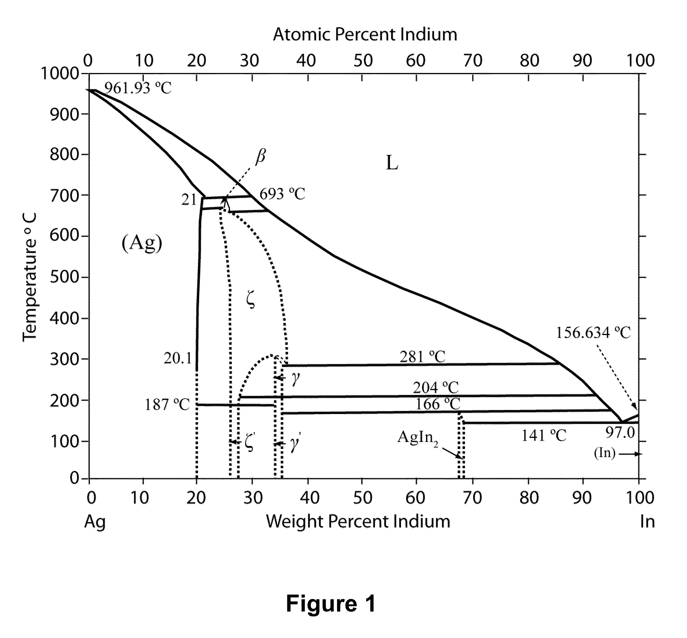
[0088]As noted above, the amount or composition of each metal to be provided in the solder material will be based upon the specific metals selected and also factors such as the desired application temperature (Ta) range over which the solder material is required to remain stable and perform according to desired specifications. An Ag—In equilibrium phase diagram is depicted in FIG. 1 and provides useful information regarding different melting points of an Ag—In alloy based upon different compositions of Ag and In in the alloy. It is preferable that a Ag—In solder material...

example 2

Forming a Solder Joint with Ag—In Solder Material

[0095]A solder joint was formed using the Ag—In solder paste material described above in Example 1 and with a TLPS process utilizing a Tp of 250° C. , a heating rate of about 1° C. / second and a holding time of 60 minutes. The solder joint was formed by applying the solder paste material to a substrate on which a TSOP package with pure Sn plated leads was to be attached. The composition of the solder joint that was formed was determined (using EDX spectrum analysis) to be about 75% by weight Ag and 25% by weight In. Any Sn dissolved from the lead finish was of such small quantity as to be undetectable by the analysis. An SEM image of the solder joint that was formed is depicted in FIG. 5. As can be seen, in particular from the magnified view of the soldered joint, generally spherical Ag particles are present and embedded within a Ag—In metal matrix.

[0096]The resultant Ag—In metal alloy forming the solder joint had a melting point of ab...

example 3

Effect of Particle Size and Holding Time on Homogenization of Ag—In Solder Material during TLPS Process

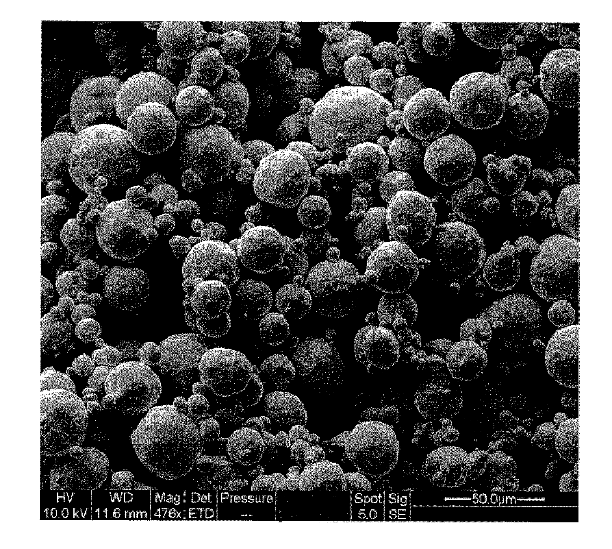
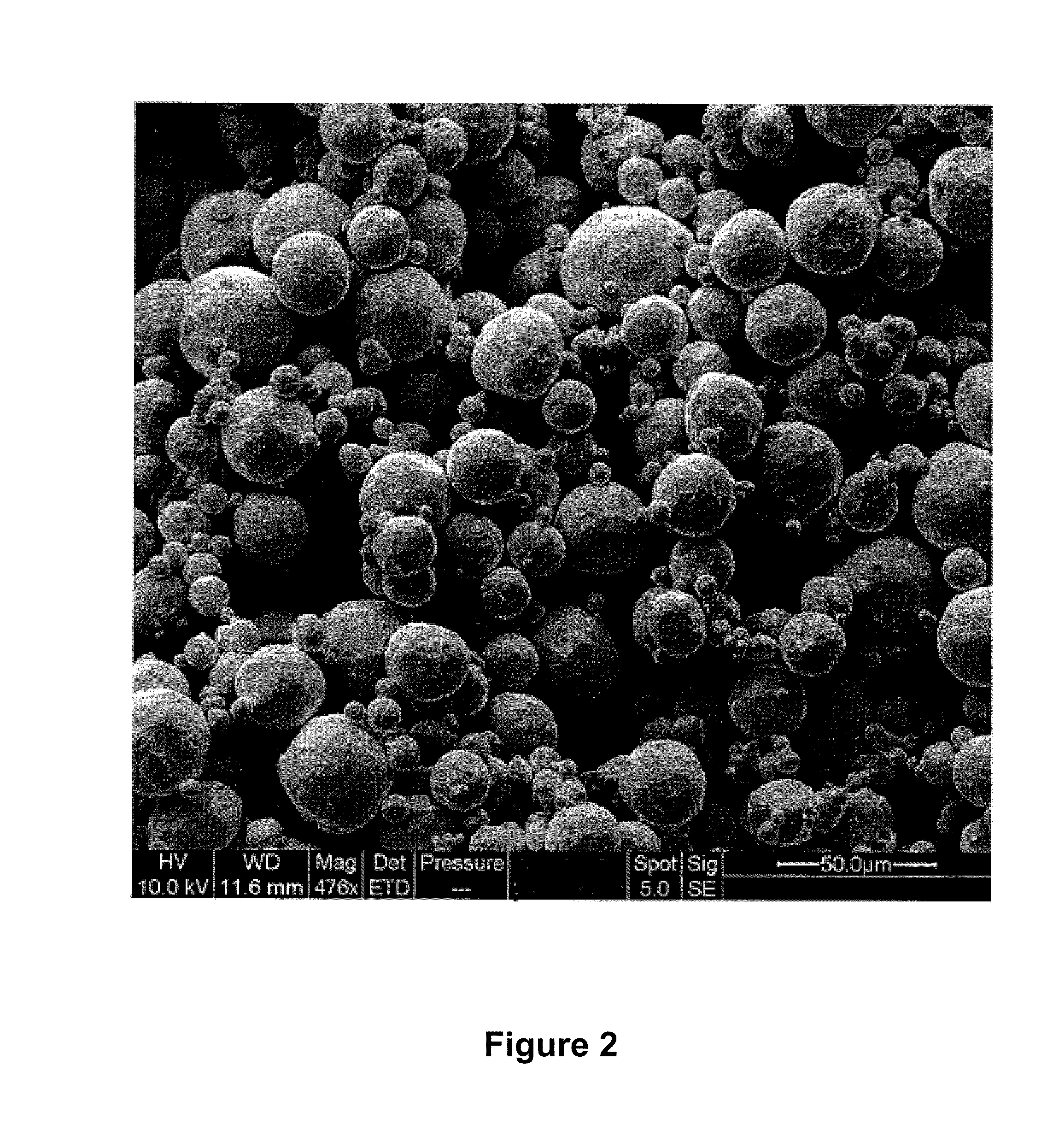
[0098]Two Ag—In solder paste materials (Paste A and Paste B) were formed in a similar manner as described above in Example 1, with the amount of Ag / In in the metal powder being about 75% Ag and about 25% In of the total metal powder weight and with a no clean RMA flux material being provided to form the paste in an amount of about 10% by total weight of the paste. In the first paste, Paste A, the nominal particle size of both Ag and In particles was limited to no more than about 25 microns (using a (−500 / +635) mesh as determined by a standard screening or sieving process, where 80% of the particles are from about 15 microns to about 25 microns). In the second paste, Paste B, the nominal particle size of both Ag and In particles was limited to no more than about 50 microns (using a (−325 / +500) mesh as determined by a standard screening or sieving process, where 80% of the particles ...


PUM

PropertyMeasurementUnit
temperatureaaaaaaaaaa
sizesaaaaaaaaaa
melting point temperatureaaaaaaaaaa

Abstract

A solder material is formed utilizing a transient liquid phase sintering process, where a precursor material is first formed. The precursor material comprises a plurality of metal particles including a first metal having a first melting point temperature and a second metal having a second melting point temperature, the first melting point temperature being greater than the second melting point temperature. The precursor material is heated to a process temperature (Tp) that is greater than the second melting point temperature and less than the first melting point temperature, and the precursor material is isothermally held at the process temperature (Tp) for a preselected holding period so as to form a metal alloy material having a melting point temperature that is greater than the process temperature. The solder material can be used to bond two components together in a device specified for use at an application temperature (Ta), where Ta/Tp>1.

Description

CROSS-REFERENCE TO RELATED APPLICATIONS [0001]This application is a continuation of U.S. patent application Ser. No. PCT / US08 / 51590 (filed Jan. 22, 2008, presently pending), which application claims priority from U.S. Provisional Patent Applications Ser. Nos. 60 / 885,997 (filed: Jan. 22, 2007, presently lapsed) and 60 / 891,763 (filed: Feb. 27, 2007, presently lapsed), all of which applications are incorporated herein by reference in their entireties.STATEMENT REGARDING FEDERALLY SPONSORED RESEARCH OR DEVELOPMENT [0002]This invention was made with Government support under W911NF0520052 awarded by Army Research Laboratory. The Government has certain rights in the invention.BACKGROUND OF THE INVENTION:[0003]1. Field of the Invention[0004]The present invention relates to solder materials for use in a bonding or attachment connection of two components.[0005]2. Description of Related Art[0006]The use of bonding materials for attaching or connecting two or more components to each other is re...

Claims


Application Information

Patent Timeline
Patent Type & Authority Applications(United States)
IPC IPC(8): B23K35/34B23K35/24
CPCB23K35/262B23K35/302B23K35/3013B23K35/3006
Inventor MCCLUSKEY, PATRICK F.QUINTERO, PEDRO
Owner UNIV OF MARYLAND
Why Eureka
Try Eureka