InGaAsSbN PHOTODIODE ARRAYS

a technology of photodiode arrays and light detection, applied in the direction of basic electric elements, electrical equipment, semiconductor devices, etc., can solve the problems of increasing the dark current by several orders of magnitude, unable to be completely eliminated, and material exhibits poor photoluminescen

Active Publication Date: 2010-04-22
TELEDYNE FLIR LLC
View PDF1 Cites 12 Cited by
  • Summary
  • Abstract
  • Description
  • Claims
  • Application Information

AI Technical Summary

Problems solved by technology

Because the material is no longer lattice-matched, dislocation defects are created in the material, which increase the dark current by several orders of magnitude over what the material should achieve theoretically.
The InAsP buffer layer 2 is used to reduce the number of defects, but they cannot be completely eliminated because they propagate through the grown layer into the absorber.
The InAsP buffer layer 2 can increase the short wavelength to 1100 nm or higher, which is undesirable because it decreases the overall wavelength range to which the detector is responsive.
However, the material exhibits poor photoluminescence which is indicative of a high concentration of defects.
By using both N and Sb added to InGaAs, an extension of the wavelength from 1.7 microns to 2.04 microns was achieved, however, previous attempts to grow this material resulted in layers that were strained, and hence limited in thickness before dislocations occur.
Therefore, they would not be useful for high-sensitivity, thick layer devices such as photodetectors.

Method used


Image

  • InGaAsSbN PHOTODIODE ARRAYS
  • InGaAsSbN PHOTODIODE ARRAYS
  • InGaAsSbN PHOTODIODE ARRAYS

Examples


Embodiment Construction

[0023]In the following description, reference is made to the accompanying drawings which form a part hereof, and which is shown, by way of illustration, several embodiments of the present invention. It is understood that other embodiments may be utilized and structural changes may be made without departing from the scope of the present invention.

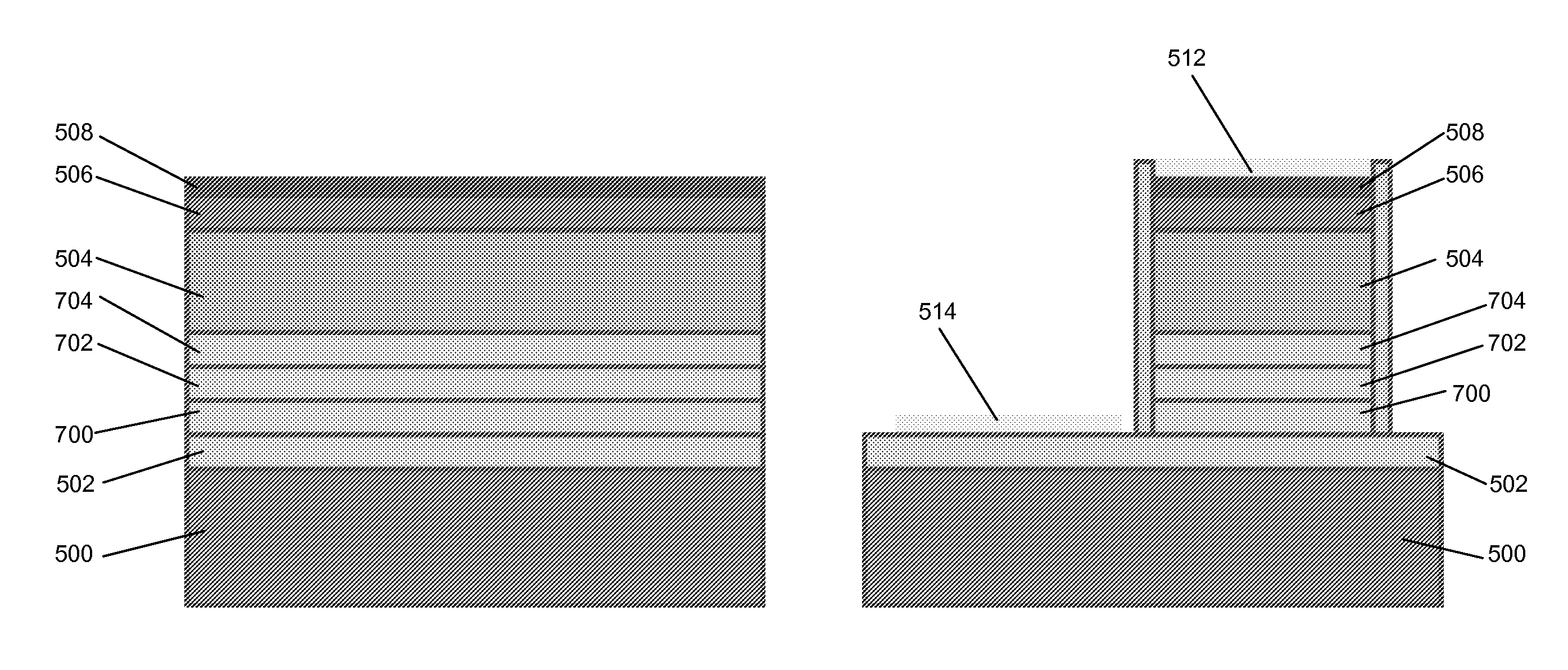
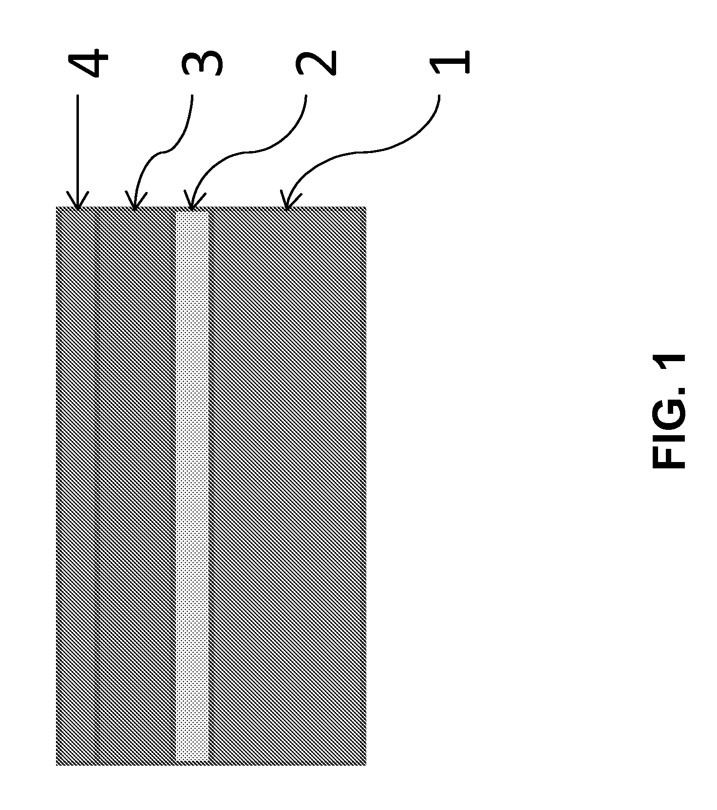
[0024]A preferred embodiment of the invention is shown in FIG. 3. An n-type InP buffer layer 6 that is 1 micron is grown on an n-type InP substrate 5. A 3.5 micron thick layer of InGaAsSbN 7 is grown on top of the buffer layer 6. Layer 7 is grown with light n-doping. A 1 micron thick InP layer 8 is grown on top of the photoabsorbing layer 7. Depending on the application, a 0.2 micron layer of InGaAs 9 is grown on top of InP layer 8 to provide a low-resistance Ohmic contact.

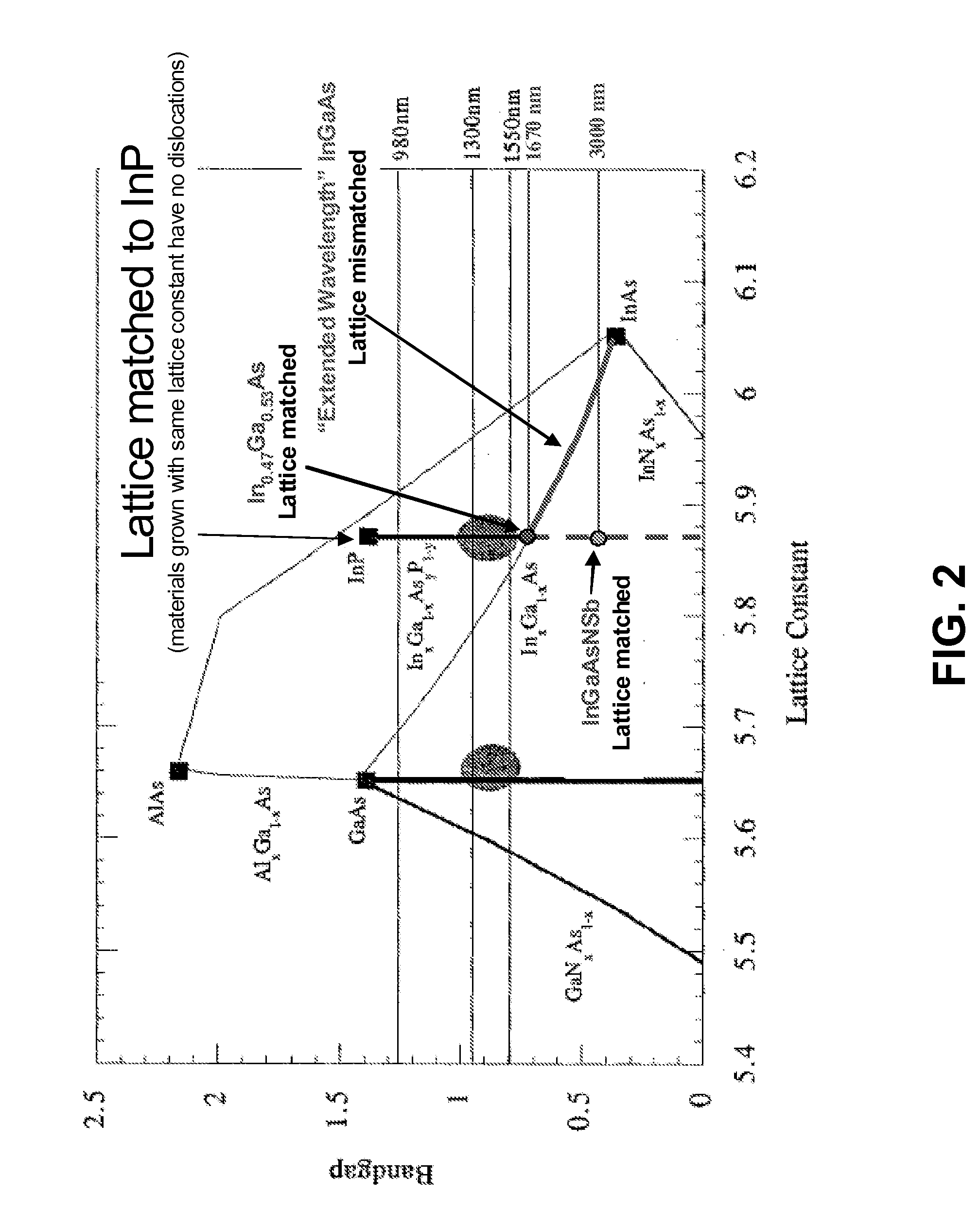
[0025]By using a preferred combination of constituent atoms, the InxGa1-xAs1-y-zSbyNz can be grown with a cutoff wavelength beyond 3 micron and still remain lattice-matche...


PUM

PropertyMeasurementUnit
thicknessaaaaaaaaaa
cutoff wavelengthaaaaaaaaaa

Abstract

Embodiments of detectors made using lattice matched photoabsorbing layers are disclosed. A photodiode apparatus in accordance with one or more embodiments of the present invention comprises an indium phosphide substrate, and a photoabsorbing region comprising at least an indium gallium arsenide antimonide nitride (InGaAsSbN) layer, wherein the InGaAsSbN layer has a thickness of at least 100 nanometers and is nominally lattice-matched to the indium phosphide substrate.

Description

BACKGROUND OF THE INVENTION[0001]1. Field of the Invention[0002]This invention relates generally to light detection and photodiode arrays, and in particular to arrays made from indium gallium arsenide and related materials.[0003]2. Description of the Related Art[0004]To extend the wavelength range of InxGa1-xAs detectors, the normal approach is to increase the Indium composition, or the x value [K. Ling a, G. Olsen, V. Ban, A. Joshi, W. Kosonocky, “Dark current analysis and characterization of InxGa1-xAs / InAsyP1-y graded photodiodes with x>0.53 for response to longer wavelengths (>1.7 microns), Journal of Lightwave Technology, vol. 10, pp. 1050-2 (1992)], which is incorporated by reference herein.[0005]FIG. 1 illustrates a description of this approach, where the substrate InP 1 has a buffer layer of InAsP 2 followed by the absorption layer InGaAs 3, followed by an InP cap 4. The InGaAs absorber 3 has a x-value that is greater than 0.53, and therefore is no longer lattice-match...

Claims


Application Information

Patent Timeline
Patent Type & Authority Applications(United States)
IPC IPC(8): H01L31/0304
CPCH01L31/03046Y02E10/544H01L31/107H01L31/105
Inventor MACDOUGAL, MICHAELGESKE, JONATHANBOWERS, JOHN E.
Owner TELEDYNE FLIR LLC
Why Eureka
Try Eureka