Fet, ferroelectric memory device, and methods of manufacturing the same

a technology of ferroelectric memory and field effect transistor, which is applied in the direction of digital storage, semiconductor devices, instruments, etc., can solve the problems of deterioration of the polarization characteristics of the ferroelectric layer b>5/b>, short data retention time of the ferroelectric memory, and poor data retention

Inactive Publication Date: 2010-04-22
UNIV OF SEOUL IND COOP FOUND
View PDF2 Cites 5 Cited by
  • Summary
  • Abstract
  • Description
  • Claims
  • Application Information

AI Technical Summary

Benefits of technology

[0009]Accordingly, the present invention has been made in an effort to solve the above-described problems. The present invention provides a field-effect transistor (FET) and a ferroelectric memory device having a simple structure and excellent data retention characteristics.

Problems solved by technology

However, the ferroelectric memory having the above-described structure has the following problems.
As a result, there occurs a problem that the polarization characteristics of the ferroelectric layer 5 are deteriorated, that is, the data retention time of the ferroelectric memory becomes very short.
However, the above MFIS type ferroelectric memory has some problems in that it requires an additional process of forming the buffer layer 20, the data retention effect is not great, and the data retention time cannot exceed 30 days even in case of an excellent product manufactured in a laboratory.

Method used


Image

  • Fet, ferroelectric memory device, and methods of manufacturing the same
  • Fet, ferroelectric memory device, and methods of manufacturing the same
  • Fet, ferroelectric memory device, and methods of manufacturing the same

Examples


Embodiment Construction

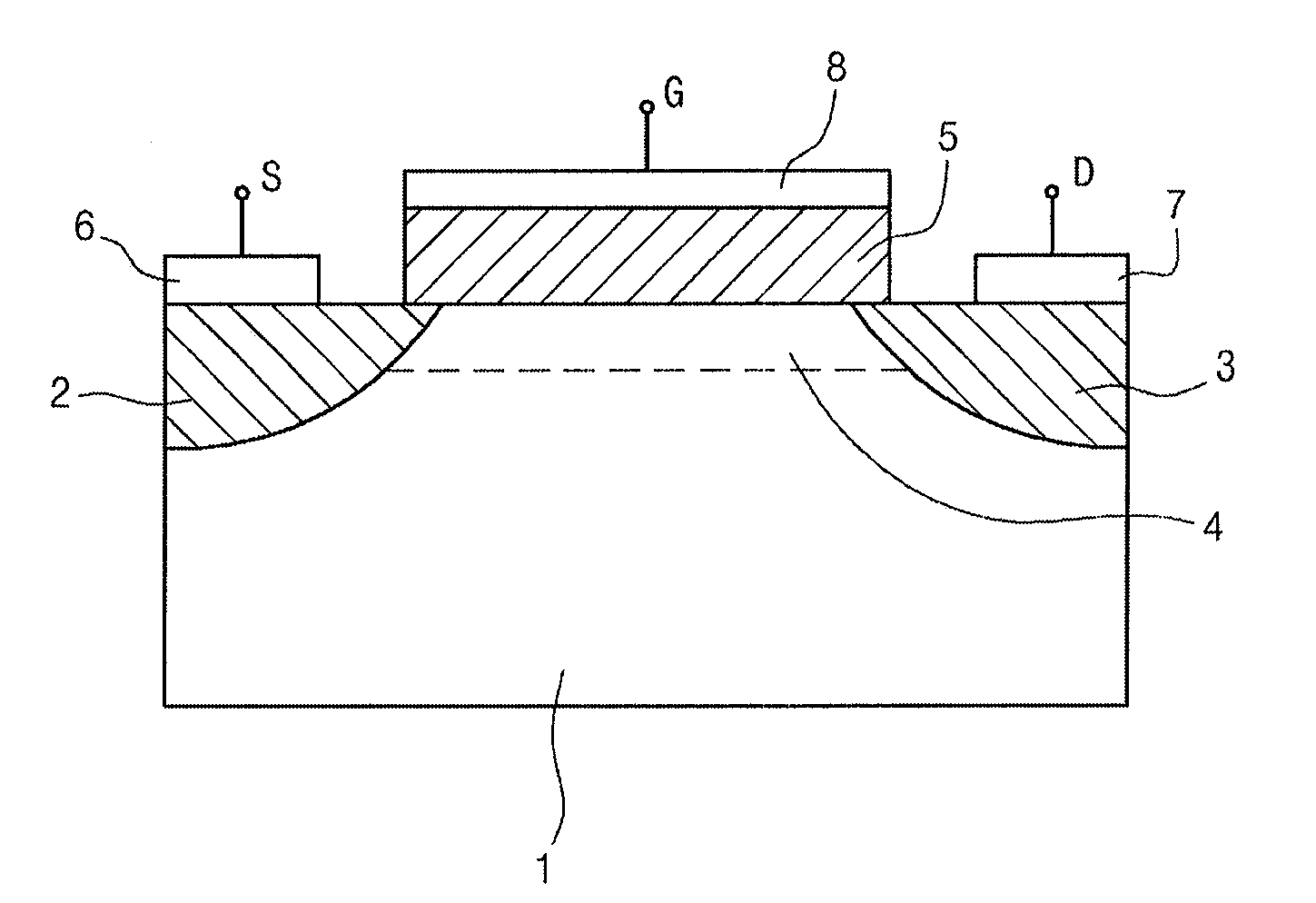
[0047]Hereinafter, preferred embodiments in accordance with the present invention will be described with reference to the accompanying drawings. The preferred embodiments are provided so that those skilled in the art can sufficiently understand the present invention, but can be modified in various forms and the scope of the present invention is not limited to the preferred embodiments.

[0048]First, the basic concept of the present invention will be described below.

[0049]At present, there are known various materials showing ferroelectric characteristics. Such materials are broadly classified into inorganic materials and organic materials. The inorganic ferroelectric materials include ferroelectric oxides, ferroelectric fluorides such as BaMgF4 (BMF), and ferroelectric semiconductors. The organic ferroelectric materials include polymer ferroelectric materials and the like.

[0050]The ferroelectric oxides include perovskite ferroelectric materials such as PbZrxTi1-xO3 (PZT), BaTiO3 and PB...


PUM

PropertyMeasurementUnit
temperatureaaaaaaaaaa
data retention timeaaaaaaaaaa
temperatureaaaaaaaaaa

Abstract

Disclosed herein are a field-effect transistor (FET), a ferroelectric memory device, and methods of manufacturing the same. The FET and the ferroelectric memory device in accordance with the present invention include: a substrate 1; source and drain regions 2 and 3 formed on the substrate; a channel layer 4 formed between the source and drain regions 2 and 3; and a ferroelectric layer 5 formed on the channel layer 4, the ferroelectric layer 5 being composed of a mixture of an inorganic ferroelectric material and an organic material. The ferroelectric layer 5 is formed in a manner that a mixed solution of an inorganic ferroelectric material and an organic material is applied onto the substrate and then subjected to annealing and etching processes.

Description

TECHNICAL FIELD [0001]The present invention relates to a field-effect transistor (FET), a ferroelectric memory device, and methods of manufacturing the same.BACKGROUND ART [0002]At present, extensive research aimed at realizing a transistor or a memory device using a ferroelectric material has continued to progress. FIG. 1 is a cross-sectional view showing a typical structure of a metal-ferroelectric-semiconductor (MFS) type memory device using a ferroelectric material.[0003]As shown in FIG. 1, source and drain regions 2 and 3 are formed in predetermined areas of a silicon substrate 1, and a ferroelectric layer 5 is formed on a channel region 4 between the source and drain regions 2 and 3. In this case, the ferroelectric layer 5 comprises an inorganic material having ferroelectric properties such as PbZrxTi1-xO3 (PZT), SrBi2Ta2O9 (SBT), (Bi,La)4Ti3O12 (BLT), and the like. Moreover, a source electrode 6, a drain electrode 7 and a gate electrode 8 formed of a metal material, respectiv...

Claims


Application Information

Patent Timeline
Patent Type & Authority Applications(United States)
IPC IPC(8): H01L29/82H01L21/8242H01L27/105
CPCG11C11/22H01L21/28291G11C11/223H01L29/40111H01L29/6684H10B51/30
Inventor PARK, BYUNG-EUN
Owner UNIV OF SEOUL IND COOP FOUND
Why Eureka
Try Eureka