Interleave control power supply device and control circuit and control method for the power supply device

a technology of power supply device and control circuit, which is applied in the direction of electric variable regulation, process and machine control, instruments, etc., can solve the problems of increasing circuit scale, long delay, and complex phase difference detection circuit, so as to prevent the reduction of phase control accuracy and improve the accuracy of phase control

Active Publication Date: 2010-04-22
FUJI ELECTRIC CO LTD
View PDF5 Cites 60 Cited by
  • Summary
  • Abstract
  • Description
  • Claims
  • Application Information

AI Technical Summary

Benefits of technology

[0091]The analog interleave control technique of the invention has no relation with variations in capacitance of capacitors and offset voltages of comparators though the background art technique has relation with such variations and offset voltages. Accordingly, phase control accuracy can be improved. Moreover, when a constant current source is used for a current, phase control accuracy can be prevented from being lowered.

Problems solved by technology

For this reason, the problem of increase in circuit scales occurs.
This causes a problem that a long delay is required before the phase difference between respective phases reaches a predetermined phase difference.
Moreover, a phase difference detecting circuit is so complex that phase control accuracy is lowered.
This causes a problem of increase in circuit scale.
There is a problem that a long time is required before the phase difference holding circuit 390 completes the phase difference control.
For this reason, there is a problem that a circuit for generating the slave signal becomes complex while phase control accuracy is low.
Particularly as for capacitors, individual variations in capacitors are unavoidable if the two capacitors are made of discrete parts.
Moreover, if an offset voltage exists in a comparator for comparing voltages of two capacitors, there is a problem that the offset voltage will directly cause error in phase difference.
With respect to the current, JP-A-10-127049 has still a problem that accuracy cannot be fully warranted because a current in a time constant circuit of CR is used.

Method used


Image

  • Interleave control power supply device and control circuit and control method for the power supply device
  • Interleave control power supply device and control circuit and control method for the power supply device
  • Interleave control power supply device and control circuit and control method for the power supply device

Examples


embodiment 1

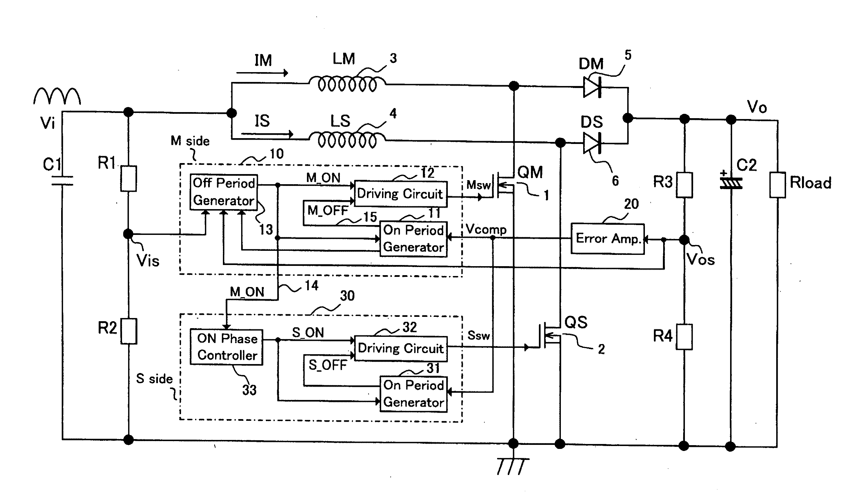
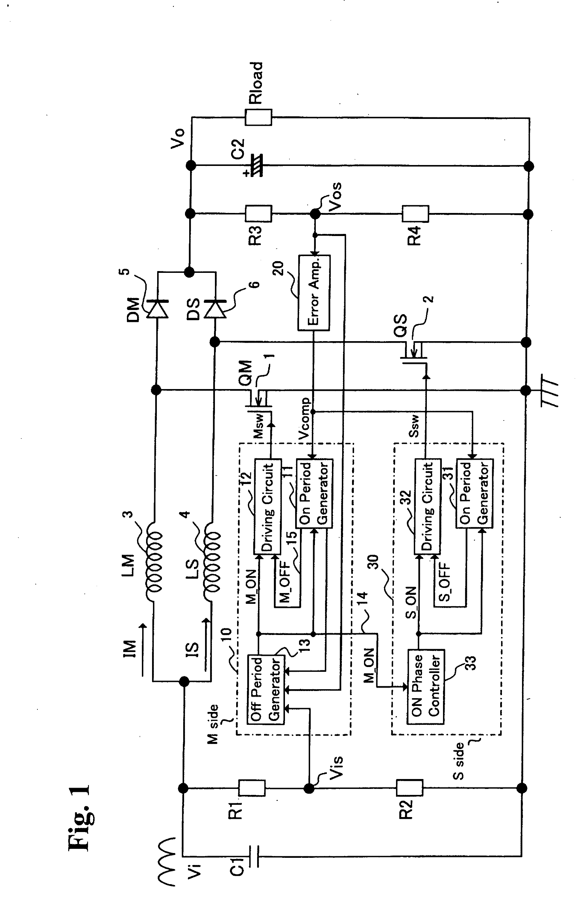
[0111]FIG. 1 is a diagram showing a circuit configuration of a two-phase critical interleaved PFC (Power Factor Correction) boost converter according to a first embodiment of the invention. The two-phase critical interleaved PFC boost converter includes a capacitor C1 for removing high-frequency noise such as switching noise superposed on an input voltage V1 which is obtained by full-wave rectifying an AC power voltage, resistors R1 and R2 for generating a voltage Vis as a detection voltage of the input voltage V1 by dividing the input voltage V1, a master-side switching element QM (1), an inductor LM (3), an anti-backflow diode DM (5), a slave-side switching element QS (2), an inductor LS (4), an anti-backflow diode DS (6), resistors R3 and R4 for generating a voltage Vos as a detection voltage of an output voltage V0 by dividing the output voltage V0, a capacitor C2 for smoothing the output voltage V0, a master-side control circuit 10 for driving the master-side switching element ...

embodiment 2

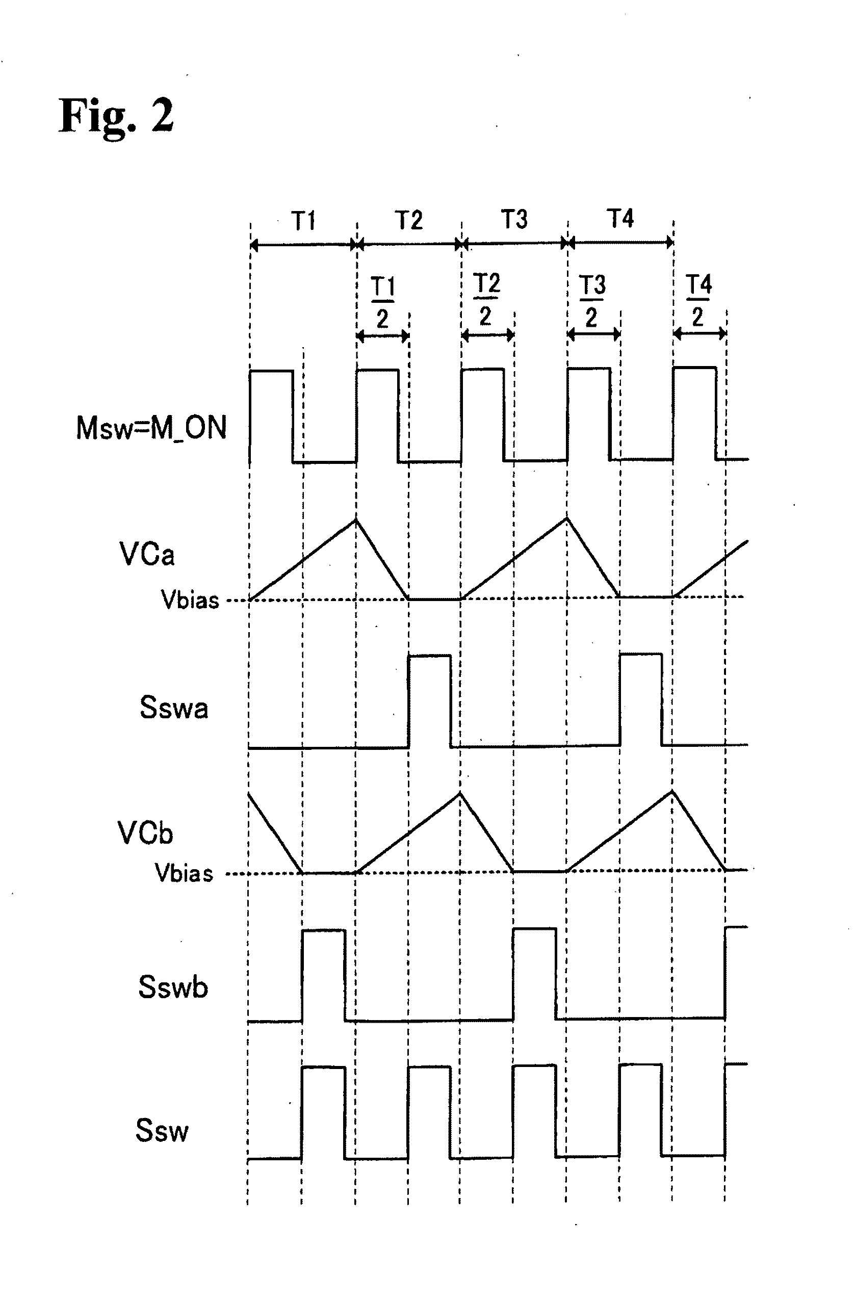
[0135]FIG. 6 is a diagram showing a circuit configuration of a two-phase critical interleaved PFC (Power Factor Correction) boost converter according to a second embodiment of the invention. The first embodiment shown in FIG. 1 has been described in the case where only the on timing of the master signal Msw is delayed, whereas the second embodiment is described in the case where an on & off phase controller determines the on / off timing of the slave signal Ssw based on the on / off timing of the master signal Msw by delaying the on / off timing of the slave signal Ssw for a half period from the on / off timing of the master signal Msw. Incidentally, the master signal Msw and the M_ON signal are equal in waveform to each other, like the first embodiment. FIG. 7 is a time chart for explaining the operation of the two-phase critical interleaved PFC boost converter shown in FIG. 6.

[0136]The circuit configuration shown in FIG. 6 is a configuration of the two-phase critical interleaved PFC boost...

embodiment 3

[0164]FIG. 10 is a diagram showing a first example of circuit configuration of a multi-phased critical interleaved PFC boost converter. FIG. 10 shows a circuit configuration obtained by increasing the number of phases in the circuit configuration of the critical interleaved PFC boost converter shown in FIG. 1 to three or more. In FIG. 10, a plurality of slave-side control circuits 301, . . . , 30m (m is an integer of 2 or more) are provided for one master-side control circuit 10. The configuration of each of the slave-side control circuits 301, . . . , 30m is the same as that of the slave-side control circuit 30 shown in FIG. 1 and detailed description thereof will be omitted here.

[0165]FIG. 11 is a diagram showing a second example of circuit configuration of the multi-phased critical interleaved PFC boost converter. FIG. 11 shows a circuit configuration obtained by increasing the number of phases in the circuit configuration of the critical interleaved PFC boost converter shown in ...


PUM


Abstract

A two-phase critical interleave PFC boost converter, includes a master-side control circuit configured to critically control a first switching element based on a master signal; and a slave-side control circuit configured to critically control a second switching element based on a slave-signal with a phase difference of 180° from the master signal. In the PFC boost converter, an off period generator of the master-side control circuit feeds an M_ON signal which is the same in waveform as the master signal to an on phase controller of the slave-side control circuit, and the slave-side control circuit determines the rising timing of the slave signal from the rising time of the master signal.

Description

BACKGROUND OF THE INVENTION AND RELATED ART STATEMENT[0001]The present invention relates to an interleave control power supply device for performing power factor correction (PFC) and a control circuit and control method for the power supply device. Particularly it relates to a switching power supply device which converts an AC power supply as an input into a DC output with a high power factor by using an interleaved switching control technique.[0002]It is well-known that AC power includes active power, reactive power and apparent power, but active power is the only power which can be converted for AC / DC conversion. Accordingly, more power can be converted into DC as the power factor is larger (close to 100%). It is therefore general that attention is paid to PFC (Power Factor Correction) when an efficient switching power supply device must be designed. In addition, PFC as a harmonic reducing circuit has become important with the advance of restrictions on harmonics in recent years.[...

Claims


Application Information

Patent Timeline
Patent Type & Authority Applications(United States)
IPC IPC(8): H02J1/00
CPCH02M2003/1586H02M3/1584H02M1/4225Y02B70/10Y02P80/10H02M3/1586
Inventor CHEN, JIAN
Owner FUJI ELECTRIC CO LTD
Why Eureka
Try Eureka