

Electronic Device and Manufacturing Method for Electronic Device
a manufacturing method and electronic device technology, applied in the field of electronic devices, to achieve the effect of improving the reliability of junctions in such electronic devices of multi-layered structures, ensuring stability, and improving junction reliability
- Summary
- Abstract
- Description
- Claims
- Application Information
AI Technical Summary
Benefits of technology
Problems solved by technology
Method used
Image

Examples
first embodiment
[0098]An electronic device manufacturing method according to a first embodiment of the invention includes: a process for setting a solder material on board electrodes of a circuit board; a process for setting resin having a flux action on electrodes of a chip component; a process for mounting the chip component onto the circuit board via the resin so that the solder material set on the board electrodes of the circuit board and the electrodes of the chip component are put into contact with each other; and a process for applying thermal energy to the solder material and the resin, whereby the method is to manufacture an electronic device in which the electrodes of the chip component are electrically connected to the board electrodes of the circuit board via the solder material and their connecting portions are sealed by the resin. This electronic device manufacturing method will be explained by taking a concrete example as Example 1 later.
[0099]Another electronic device manufacturing ...
example 1
[0110]An example in which an electronic component (chip component) with no solder bumps added thereon such as resistors or other electronic components is mounted on an electronic circuit board via solder material will now be explained with reference to the accompanying drawings.
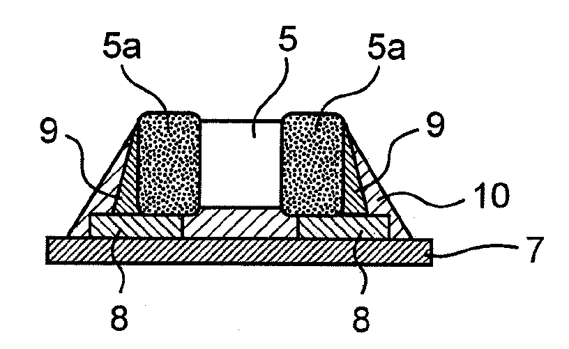
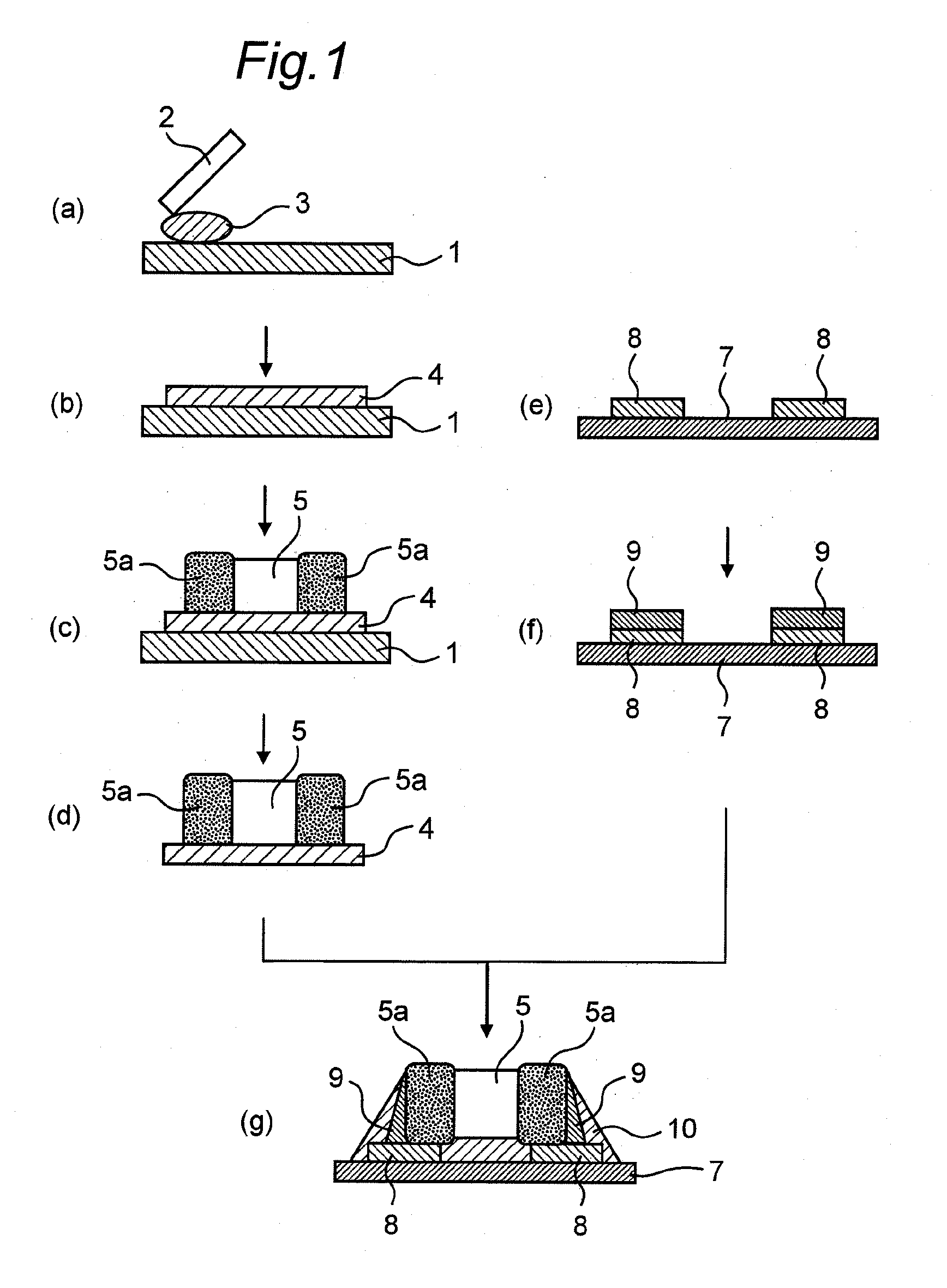
[0111]FIG. 1 is a view relating to a mounting method for a chip component 5, which is an electronic component, in Example 1 of the invention.
[0112]A resin 3 having the flux action was thrown onto a material pot 1 (FIG. 1(a)). Next, with use of a squeegee 2, a layer of a resin 4 having the flux action and having a certain film thickness was formed (FIG. 1(b)). Next, for transfer of the resin 3 having the flux action, the chip component 5 was mounted on the layer of the resin 4 having the flux action and having a certain film thickness (FIG. 1(c)). By pull-up of the mounted chip component 5, a chip component 5 onto which a necessary amount of the resin 3 (i.e., resin layer) having the flux action had been trans...
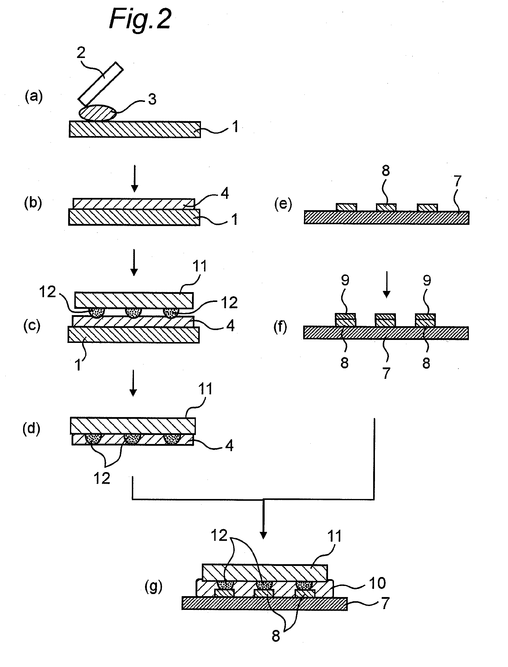
example 2
[0129]As Example 2 of the invention, a method in which a bump-added electronic component as an example of the second circuit assembly is mounted on an electronic circuit board as an example of the first circuit assembly will now be explained below with reference to the accompanying drawings. FIGS. 2(a) to 2(g) are views relating to the mounting method for bump-added electronic components in Example 2 of the invention.
[0130]A resin 3 having the flux action was thrown onto a material pot 1 (FIG. 2(a)). Next, with use of a squeegee 2, a layer of a resin 4 having the flux action and having a certain film thickness was formed (FIG. 2(b)). Next, for transfer of the resin 3 having the flux action, a bump-added electronic component (BGA 11) was mounted on the layer of the resin 4 having the flux action and having a certain film thickness (FIG. 2(c)). By pull-up of the mounted bump-added electronic component, a bump-added electronic component (BGA 11) onto which the resin 4 having the flux a...
PUM
| Property | Measurement | Unit |
|---|---|---|
| Length | aaaaa | aaaaa |
| Length | aaaaa | aaaaa |
| Length | aaaaa | aaaaa |
Abstract
Description
Claims
Application Information