

Semiconductor memory with reed-solomon decoder
a technology of reed-solomon decoder and memory device, which is applied in the field of error checking/correction system, can solve the problems of increasing error rate, increasing error rate, and increasing error ra
- Summary
- Abstract
- Description
- Claims
- Application Information
AI Technical Summary
Benefits of technology
Problems solved by technology
Method used
Image

Examples
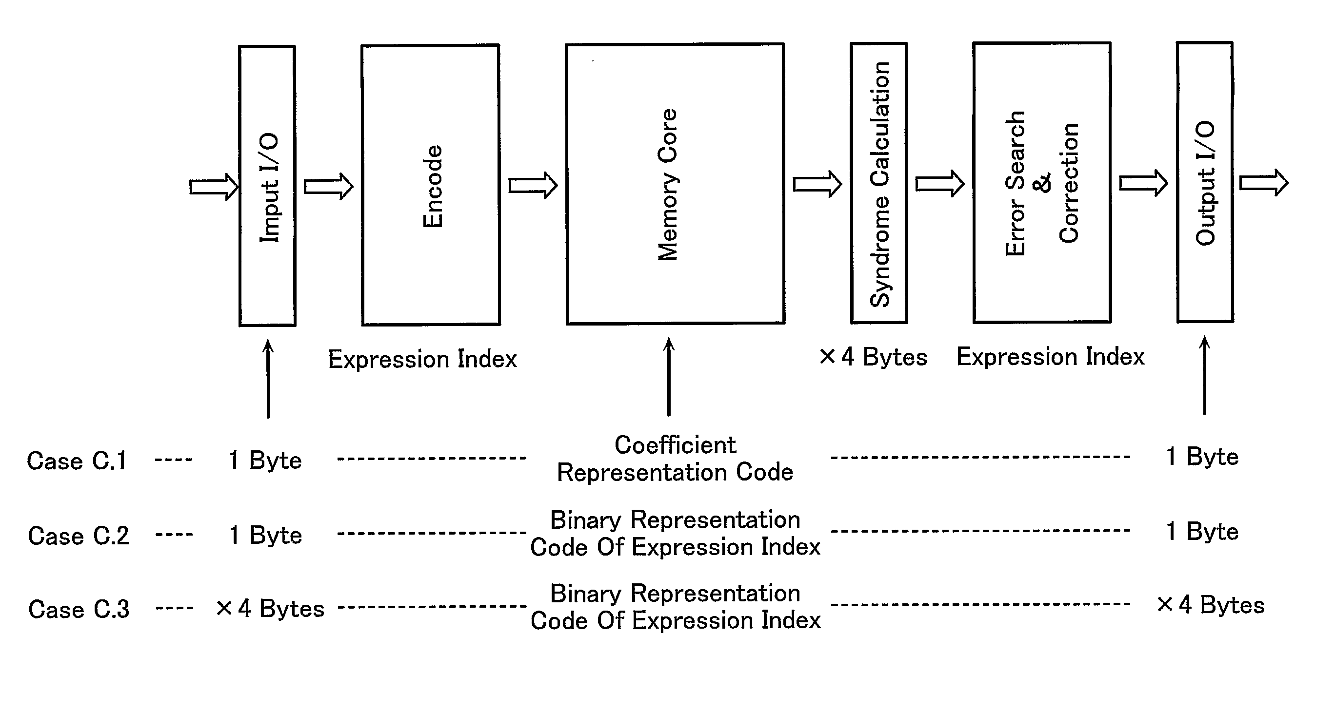
case c.1
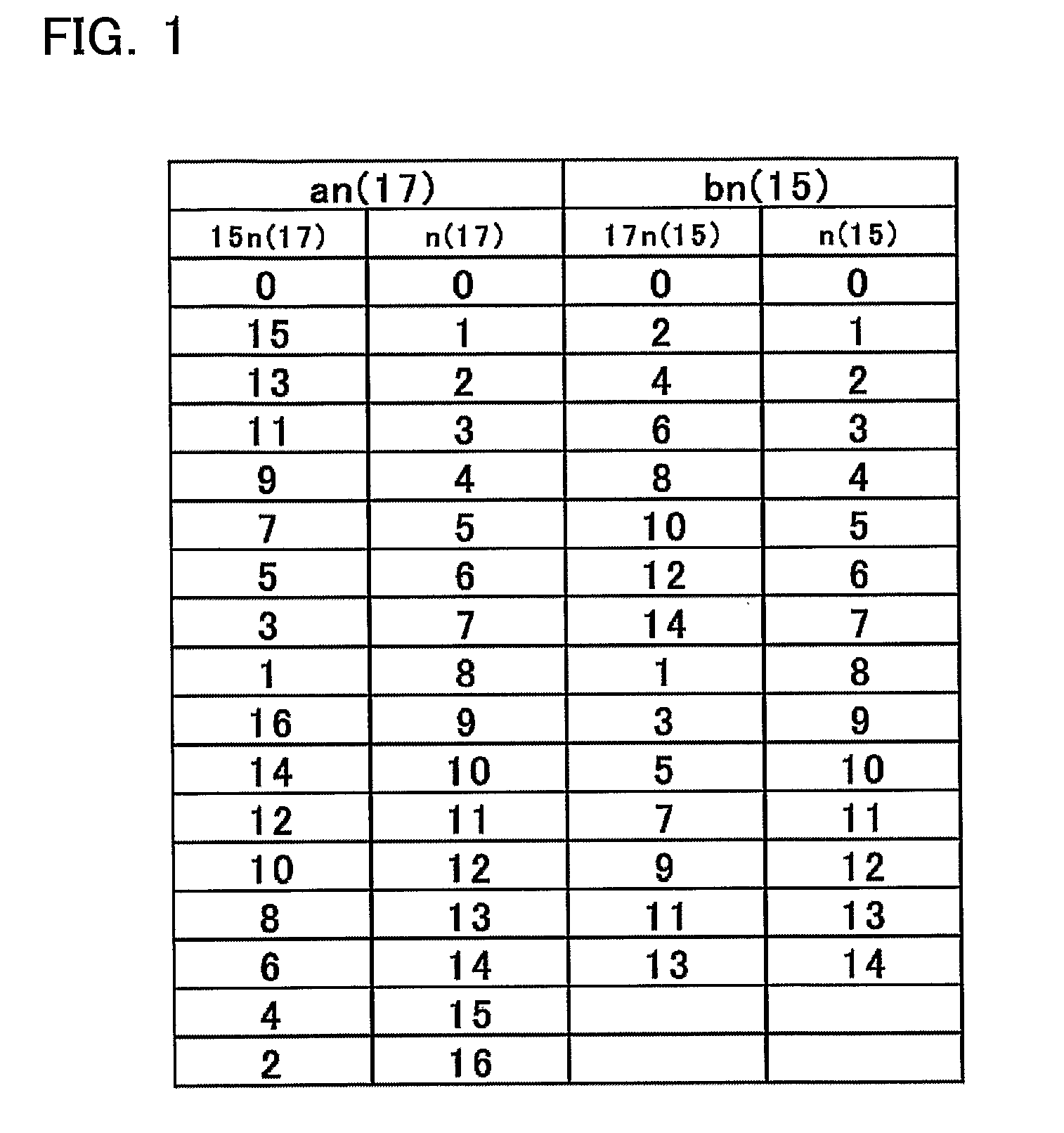
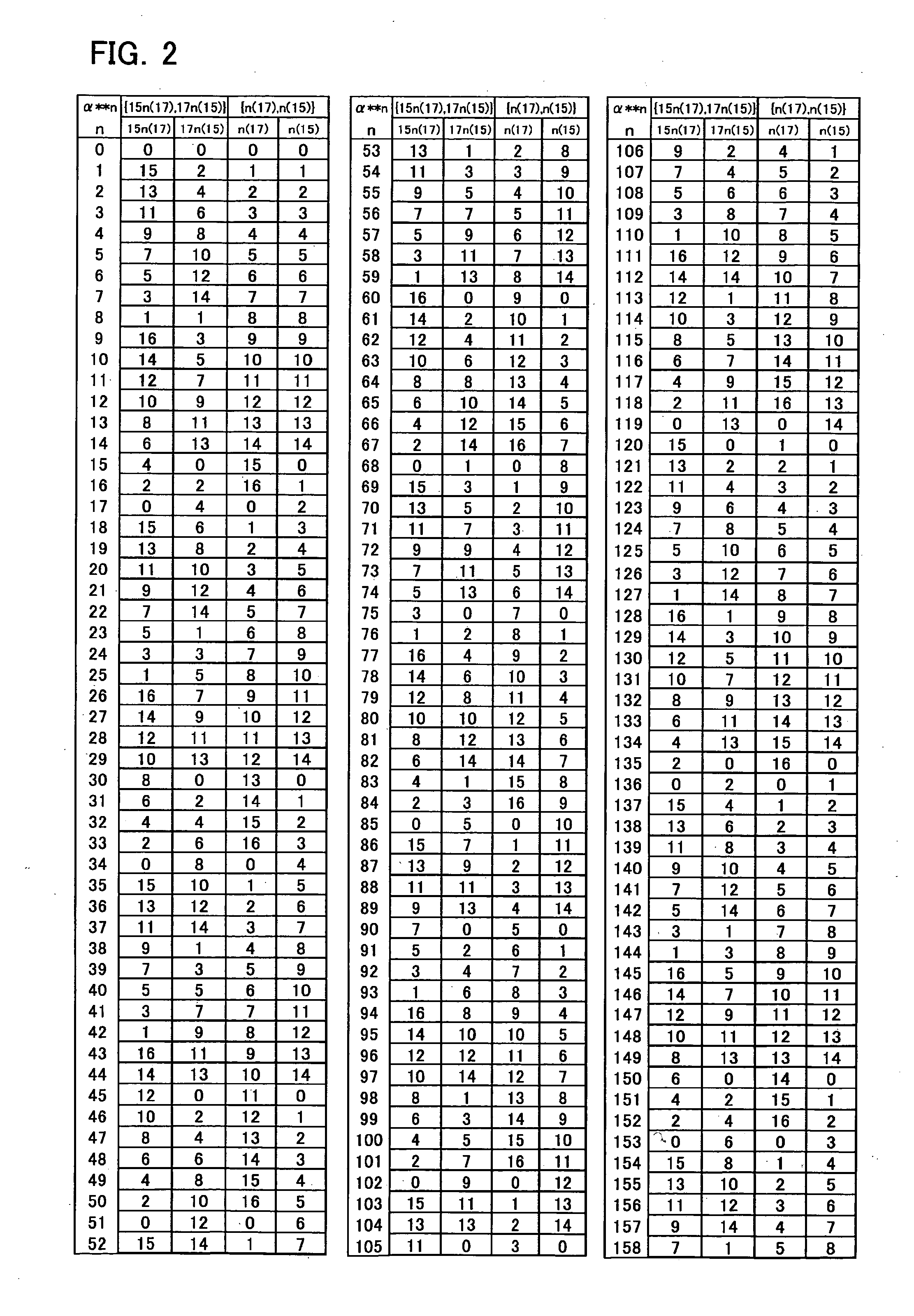
[0246 . . . . External data is regarded on a byte basis as an element in GF(256) or a coefficient of a seventh order irreducible residue polynomial pn(x) and is subjected to a code computation. Data to be stored in the memory is symbolized on a byte basis as a coefficient of the residue polynomial pn(x). In the description of the case C.1, basic methods of encoding and decoding are described.
case c.2
[0247 . . . . A method for reducing the number of decoding circuits between coefficient representations of pn(x) and index representations, or the parts having the largest circuitry scale in the case C.1. External data is regarded as a binary representation of an expression index of an element in GF(256) to increase the parts that can be computed without decoding.
[0248]A symbol is stored in the memory on a byte basis as a binary representation of an expression index. The case C.2 is described only on the parts changed from the case C.1.
case c.3
[0249 . . . . In the cases C.1, C.2, data is exchanged on a byte basis between the ECC system and the outside on the assumption that a data block simultaneously processed at ECC is read into the memory in 16 cycles. It may be required, however, to increase the bandwidth for data transfer with simultaneous processing of 2 bytes or more. Therefore, as an example of multi-byte simultaneous transfer or a method of exchanging data on a 4-byte basis is used as the case C.3, or as a modification of the case C.2 scheme, an interface configuration is described.
[Description of Case C.1
[0250]First, the case C.1 is described in detail.
(Data Encoding Unit)
[0251]The following description is given to a method of creating from external data a code polynomial c(x) having a coefficient that is code data to be stored in the memory.
[0252]The external data is symbolized at every 8 bits (=1 byte). In order to associate a coefficient ai of the information data polynomial f(x) with a finite field element a...
PUM
 Abstract
Description
Claims
Application Information