Semiconductor integrated circuit device for driving display device and manufacturing method thereof

Inactive Publication Date: 2010-05-13
RENESAS ELECTRONICS CORP
View PDF6 Cites 28 Cited by
  • Summary
  • Abstract
  • Description
  • Claims
  • Application Information

AI Technical Summary

Benefits of technology

[0012]In semiconductor integrated circuit devices (for example, LCD driver IC) having a driver for driving a display device such as LCD (Liquid Crystal Display), COG (Chip On Glass) packaging is employed for chip packaging. In order to achieve this, an elongate and relatively thick gold bump electrode, for example, having a width of about 10 μm, length of about 150 μm, and thickness of about 15 μm is formed over an aluminum-based bonding pad having a relatively small

Problems solved by technology

In consideration of narrowing tendency of the pitch between gold bump elect

Method used


Image

  • Semiconductor integrated circuit device for driving display device and manufacturing method thereof
  • Semiconductor integrated circuit device for driving display device and manufacturing method thereof
  • Semiconductor integrated circuit device for driving display device and manufacturing method thereof

Examples


embodiments

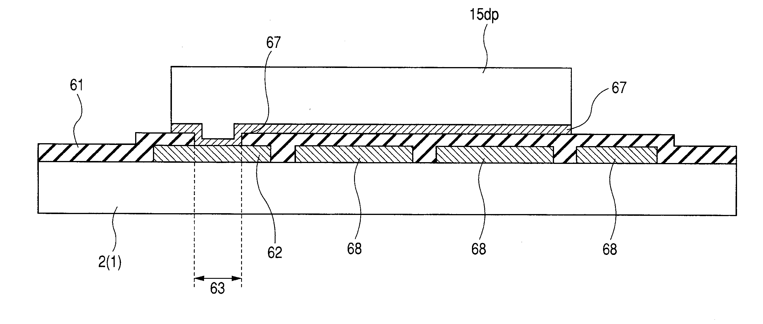
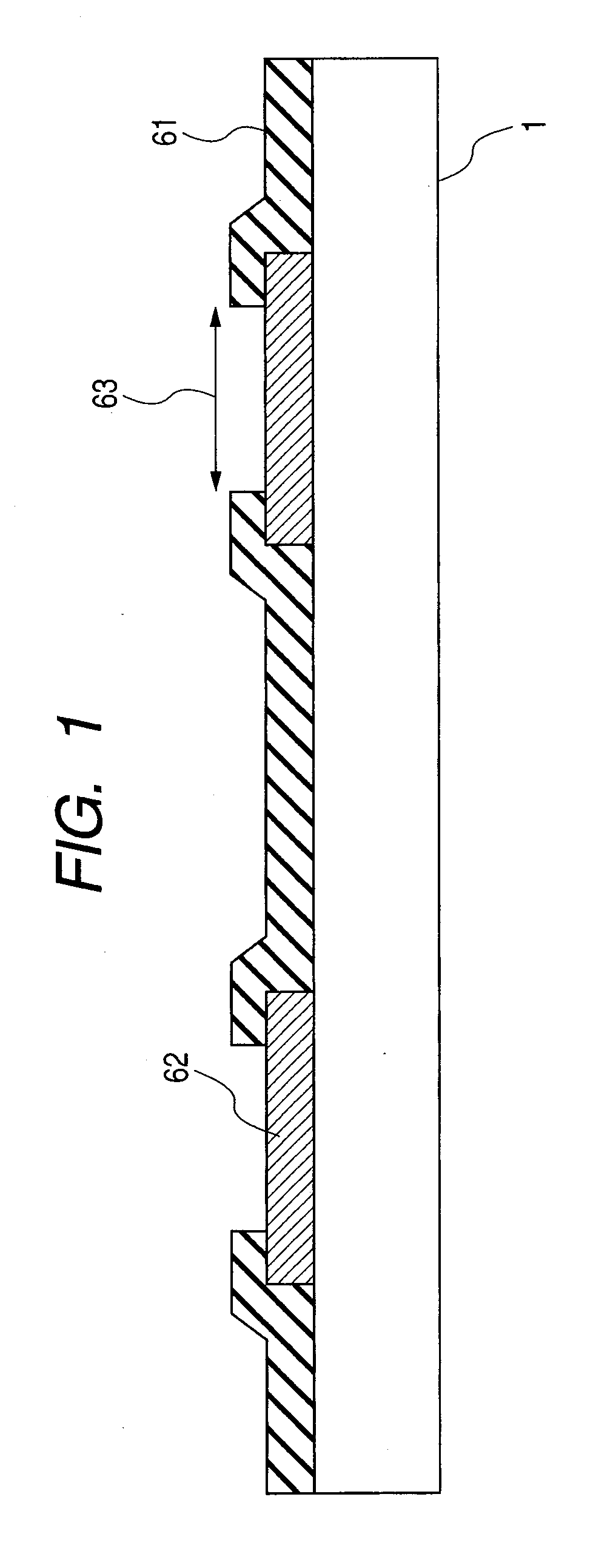
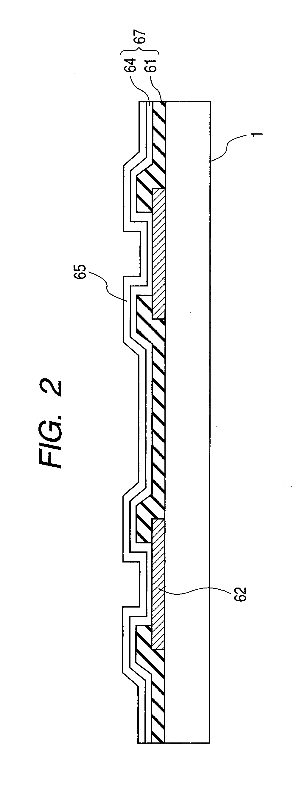
[0082]The embodiments of the invention will hereinafter be described specifically. In all the drawings, the same or like members will be identified by the same or like symbols or reference numerals and overlapping descriptions will be omitted in principle.

[0083]Sections 1 to 3 are mainly related to the first layout of drive output bump electrodes (in which the bump electrodes have the following relationship in width: outer drive output bump electrodes


PUM


Abstract

A semiconductor integrated circuit device for driving an LCD, COG chip packaging is performed. To achieve this, an elongate and relatively thick gold bump electrode is formed over an aluminum-based pad having a relatively small area. In a wafer probe test performed after formation of the gold bump electrode, a cantilever type probe needle having gold as a main component and having an almost perpendicularly bent tip portion is used. The diameter of this probe needle in the vicinity of its tip is usually almost the same as the width of the gold bump electrode. This makes it difficult to perform the wafer probe test stably. To counteract this, a plurality of bump electrode rows for outputting a display device drive signal are formed such that the width of inner bump electrodes is made greater than the width of outer bump electrodes.

Description

CROSS-REFERENCE TO RELATED APPLICATIONS[0001]The disclosure of Japanese Patent Application No. 2008-289570 filed on Nov. 12, 2008 including the specification, drawings and abstract is incorporated herein by reference in its entirety.BACKGROUND OF THE INVENTION[0002]The present invention relates to the structure of a bonding pad group in a semiconductor integrated circuit device and a technology effective when applied to a wafer testing technology in a manufacturing method of a semiconductor integrated circuit device (or a semiconductor device).[0003]Japanese Unexamined Patent Publication No. 2002-196353 (Patent Document 1) or U.S. Pat. No. 6,678,028 (Patent Document 2) corresponding thereto discloses a technology of, in an LSI (Large Scale Integration) device chip for LCD (Liquid Crystal Display) driver, laying out two rows of bonding pad groups in such a manner that bonding pads of the bonding pad group belonging to the row close to the edge portion of the chip have an elongate sha...

Claims


Application Information

Patent Timeline
IPC IPC(8): H01L33/00H01L23/498H01L23/58H01L21/66
CPCG01R31/318511G09G3/006G09G3/3648G09G2300/0426H01L24/14H01L24/17H01L25/16H01L2224/0345H01L2224/0361H01L2224/05027H01L2224/05124H01L2224/05166H01L2224/05572H01L2224/05664H01L2224/11462H01L2224/1147H01L2224/11912H01L2224/13013H01L2224/13016H01L2224/13027H01L2224/13144H01L2224/1403H01L2224/14051H01L2224/83851H01L2224/9211H01L2924/01013H01L2924/01015H01L2924/01022H01L2924/01027H01L2924/01029H01L2924/01046H01L2924/01049H01L2924/01074H01L2924/01078H01L2924/01079H01L2924/01082H01L2924/14H01L2924/19041H01L24/13H01L2924/01005H01L2924/01006H01L2924/01033H01L2924/01047H01L23/48H01L2224/29299H01L2224/29399H01L2224/02166H01L2224/05553H01L2224/05554H01L2224/0603H01L2224/0401H01L2924/1461H01L2924/00014H01L2924/0002H01L2224/81H01L2924/00H01L2224/05552H01L2924/15788
Inventor OBUCHI, ATSUSHIHIGUCHI, KAZUHISAOKADO, KAZUOMITSUI, KAZUTOMIYATA, SHUSAKU
Owner RENESAS ELECTRONICS CORP
Why Eureka
Try Eureka