Method of Forming Insulation Film Using Plasma Treatment Cycles

Active Publication Date: 2010-05-20
ASM JAPAN
View PDF7 Cites 438 Cited by
  • Summary
  • Abstract
  • Description
  • Claims
  • Application Information

AI Technical Summary

Benefits of technology

[0007]In a representative example of the present invention, a film of good film qua

Problems solved by technology

However, films formed at low temperature present a problem in that they have a very high wet etching rate (WER).
However, neither of them

Method used


Image

  • Method of Forming Insulation Film Using Plasma Treatment Cycles
  • Method of Forming Insulation Film Using Plasma Treatment Cycles
  • Method of Forming Insulation Film Using Plasma Treatment Cycles

Examples


Example

Example 1

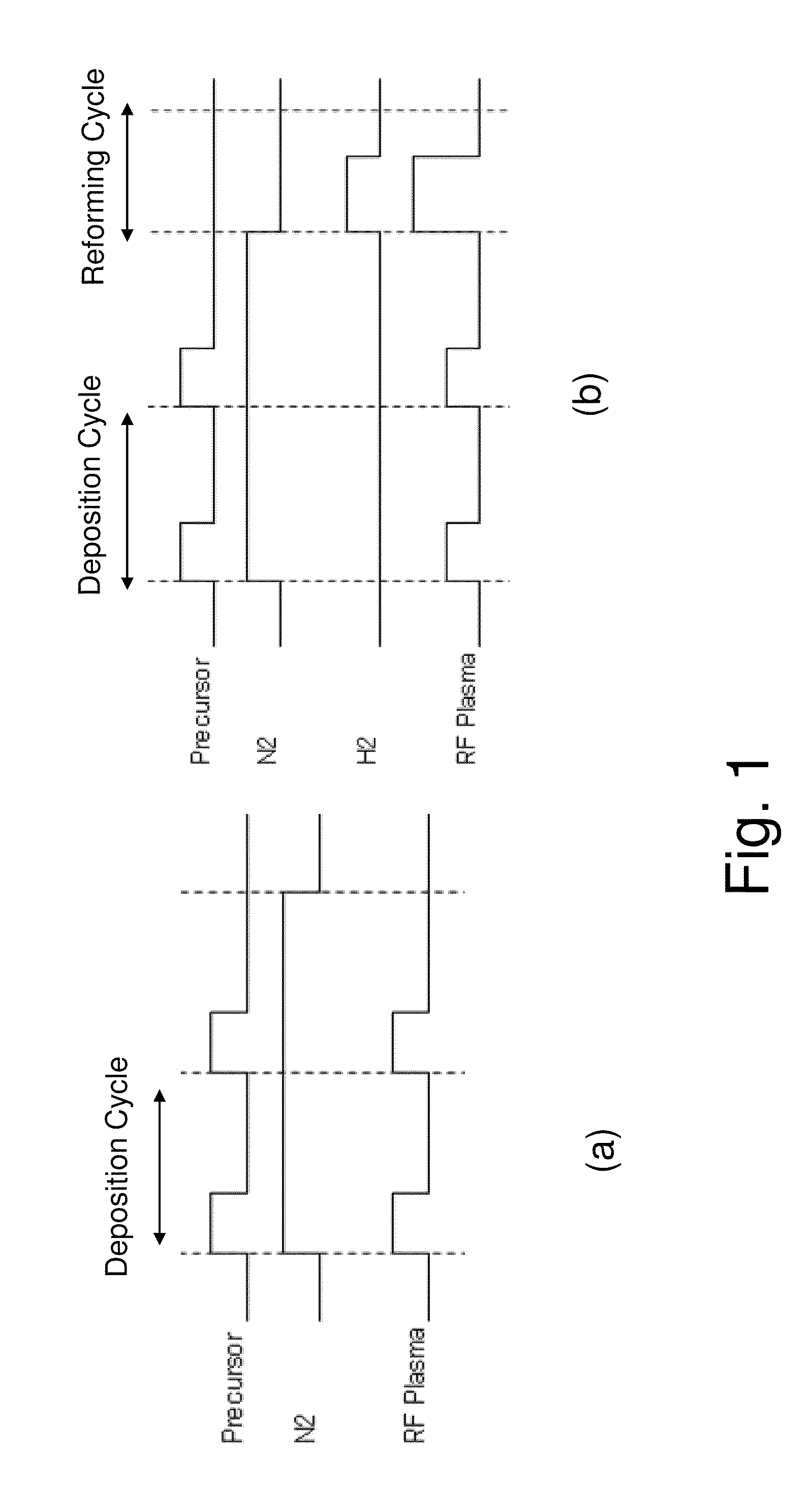
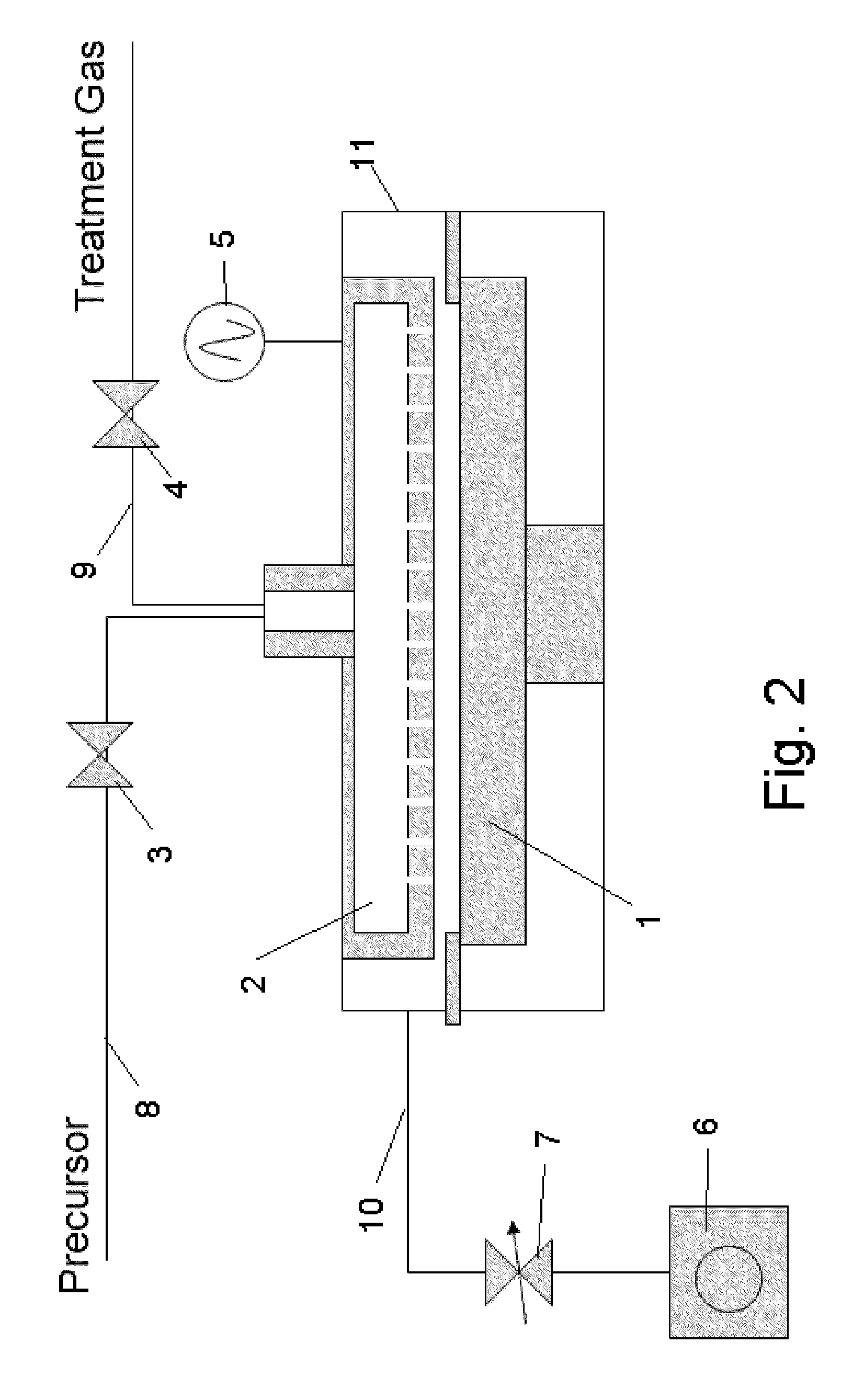
[0063]In this example, the apparatus shown in the schematic diagram of FIG. 2 was used to form a film. This apparatus comprises a reactor 11 which can be retained in a vacuum state, susceptor 1 with heating mechanism used to hold a wafer on top, shower head 2 which provides a mechanism for supplying gas, RF application mechanism 5 that generates a plasma between the shower head and susceptor, the material gas supply line equipped with an open / close valve 3 connected to the shower head 2, treating gas supply line 9 equipped with another open / close valve 4, exhaust line 10 used to exhaust the atmosphere inside the reactor 11, and vacuum pump 6 connected after the exhaust line via a pressure control valve 7, among others. Note that a purge gas line (not illustrated) is also connected to the shower head 2 just like the reactant gas supply line 9.

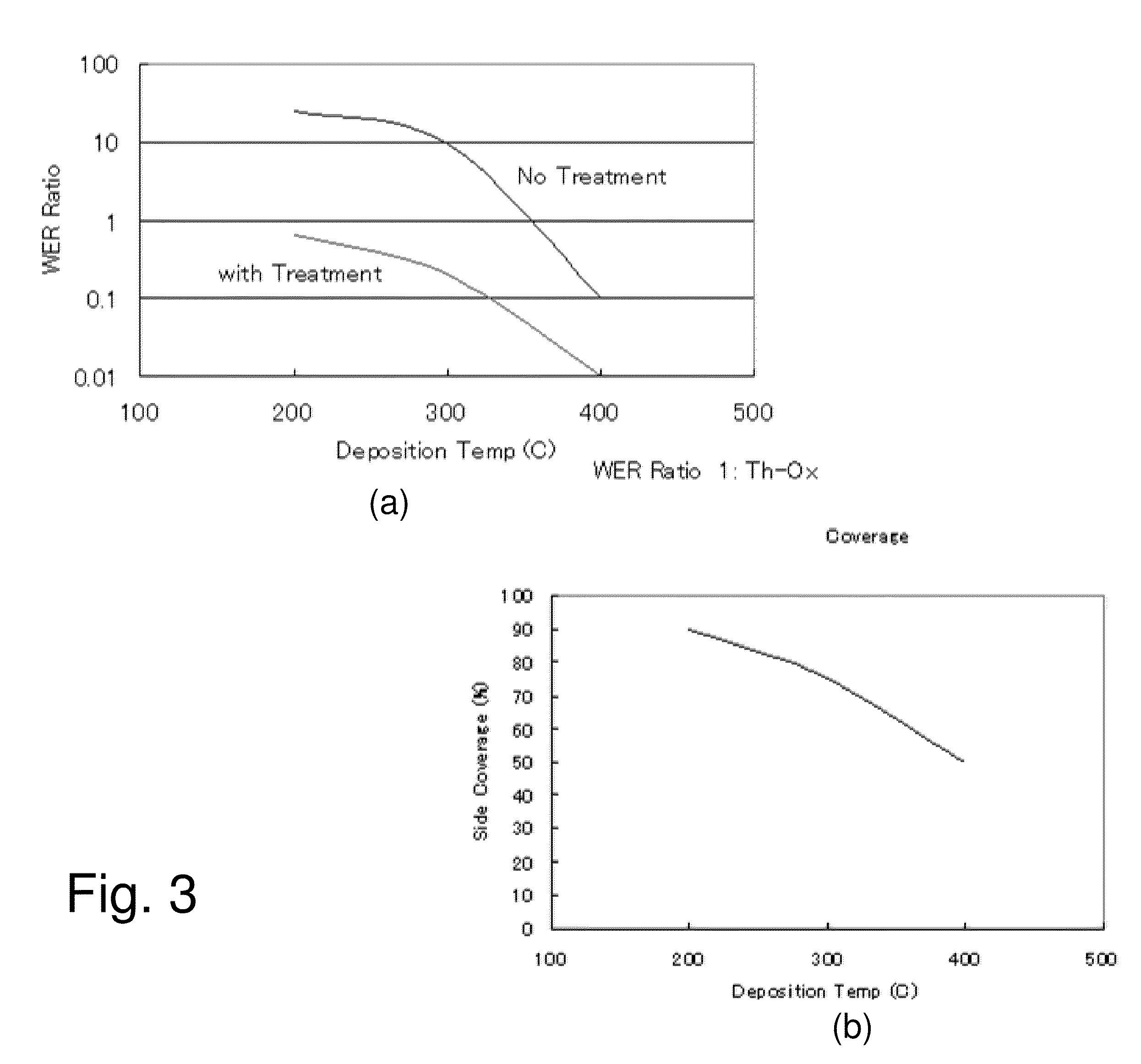
[0064]A Si wafer (300 mm in diameter) was heated to 200° C., and then (a) 3DMAS SiH[NMe2]3, N2 and H2 were supplied and RF was applied...

Example

Example 2

[0066]A film was formed in the same manner as in Example 1, except that NH3 was supplied (by 300 sccm) instead of H2, in the reforming process. While the SiN film in Example 1 was obtained as a result of the reforming effect achieved by H2 plasma, a similar reforming effect (low WER) was also achieved in the present example using NH3 plasma instead of H2 plasma.

Example

Example 3

[0067]In accordance with Example 1, a film was formed by CVD using 4MS (tetramethyl silane) being the material and NH3 at a film forming temperature of 550° C. and RF power of 50 W, after which a reforming cycle was implemented in which Ar was supplied (by 500 sccm) and RF power was applied. Examples of sequences are shown in FIG. 5 (7), (8). In (7), 600 W was applied when Ar was supplied, while in (6), 30 W was applied in the reforming cycle. While the WER at 1% HF was 60 nm / min without reforming cycle, it improved dramatically to 0.1 nm / min with reforming at 600 W and also to a plausible 1 nm / min with reforming at 30 W. In other words, good improvement characteristics could be achieved by using Ar gas. Similar results were also achieved when Xe gas was used. The difference in film thickness was 5% or less, when comparing the case of reforming process and the case of no reforming process. The WER improved significantly in a similar sequence at a film forming temperature of...


PUM

PropertyMeasurementUnit
Timeaaaaaaaaaa
Frequencyaaaaaaaaaa

Abstract

A film forming cycle based on pulse CVD or ALD is repeated multiple times to form a single layer of insulation film, while a reforming cycle is implemented in the aforementioned process, either once or multiple times per each film forming cycle, by treating the surface of formed film using a treating gas that has been activated by a plasma.

Description

CROSS REFERENCE TO RELATED APPLICATIONS[0001]This application claims the benefit of U.S. Provisional Application No. 61 / 114,879, filed Nov. 14, 2008, and the disclosure of which is herein incorporated by reference in its entirety.BACKGROUND[0002]1. Field of the Invention[0003]The present invention generally relates to a method of forming an insulation film by pulse plasma chemical vapor deposition (pulse CVD) or atomic layer deposition (ALD).[0004]2. Description of the Related Art[0005]SiN films used as gate spacers must offer a good coverage and have an etch rate equivalent to or less than thermal oxide films. A general rule of thumb is that the lower the film forming temperature, the better the coverage. However, films formed at low temperature present a problem in that they have a very high wet etching rate (WER). For example, a sequence based on the conventional pulse CVD is shown in FIG. 1(a). A similar pattern is also seen when ALD is used.SUMMARY[0006]In an embodiment of the ...

Claims


Application Information

Patent Timeline
IPC IPC(8): B05D3/04
CPCC23C16/345C23C16/56C23C16/45542
Inventor KOBAYASHI, AKIKOSHIMIZU, AKIRAHONG, KUO-WEIKOBAYASHI, NOBUYOSHIFUKAZAWA, ATSUKI
Owner ASM JAPAN
Why Eureka
Try Eureka