Process for Preparing Substituted Pentacenes

a pentacenes and process technology, applied in the field of process for preparing substituted pentacenes, can solve the problems of difficult control, complex method, and high cost of vapour deposition equipmen

Active Publication Date: 2010-05-27
FLEHKSENEHBL LTD
View PDF1 Cites 14 Cited by
  • Summary
  • Abstract
  • Description
  • Claims
  • Application Information

AI Technical Summary

Benefits of technology

[0029]Said components and devices include, without limitation, electrooptical displays, LCDs, optical films, retarders, compensators, polarisers, beam splitters, reflective films, alignment layers, colour filters, holographic elements, hot stamping foils, coloured images, decorative or security markings, LC pigments, adhesives, non-linear optic (NLO) devices, optical information storage devices, electronic devices, organic semiconductors, organic field effect transistors (OFET), integrated circuits (IC), thin film transistors (TFT), Radio Frequency Identification (RFID) tags, organic light emitting diodes (OLED), organic light emitting transistors (OLET), electroluminescent displays, organic photovoltaic (OPV) devices, organic solar cells (O-SC), organic laser diodes (O-laser), organic integrated circuits (O-IC), lighting devices, sensor devices, electrode materials, photoconductors, photodetectors, electrophotographic recording devices, capacitors, charge injection layers, Schottky diodes, planarising layers, antistatic films, conducting substrates, conducting patterns, photoconductors, electrophotographic applications, electrophotographic recording, organic memory devices, biosensors, biochips.

Problems solved by technology

Thus, in the prior art, thin films of pentacene have been vapour deposited, due in part to the fact that pentacene is rather insoluble in common solvents.
However, vapour deposition requires expensive and sophisticated equipment.
However, the latter method is also complex and it is difficult to control in order to obtain the necessary ordered structure for good charge mobility.
However, the properties of the bis(silylethynyl)pentacenes described in prior art still leave room for further improvement.
However, it was also found that such substituted pentacenes are difficult to synthesize.
However, the inventors have found that for 1,4,8,11-tetrasubstituted 6,13-bis(triethylsilylethynyl) pentacene both the Aldol and Cava methodologies yield little success in constructing the pentacene ring-network precursors in high and reproducible yields.

Method used


Image

  • Process for Preparing Substituted Pentacenes
  • Process for Preparing Substituted Pentacenes
  • Process for Preparing Substituted Pentacenes

Examples


example 1

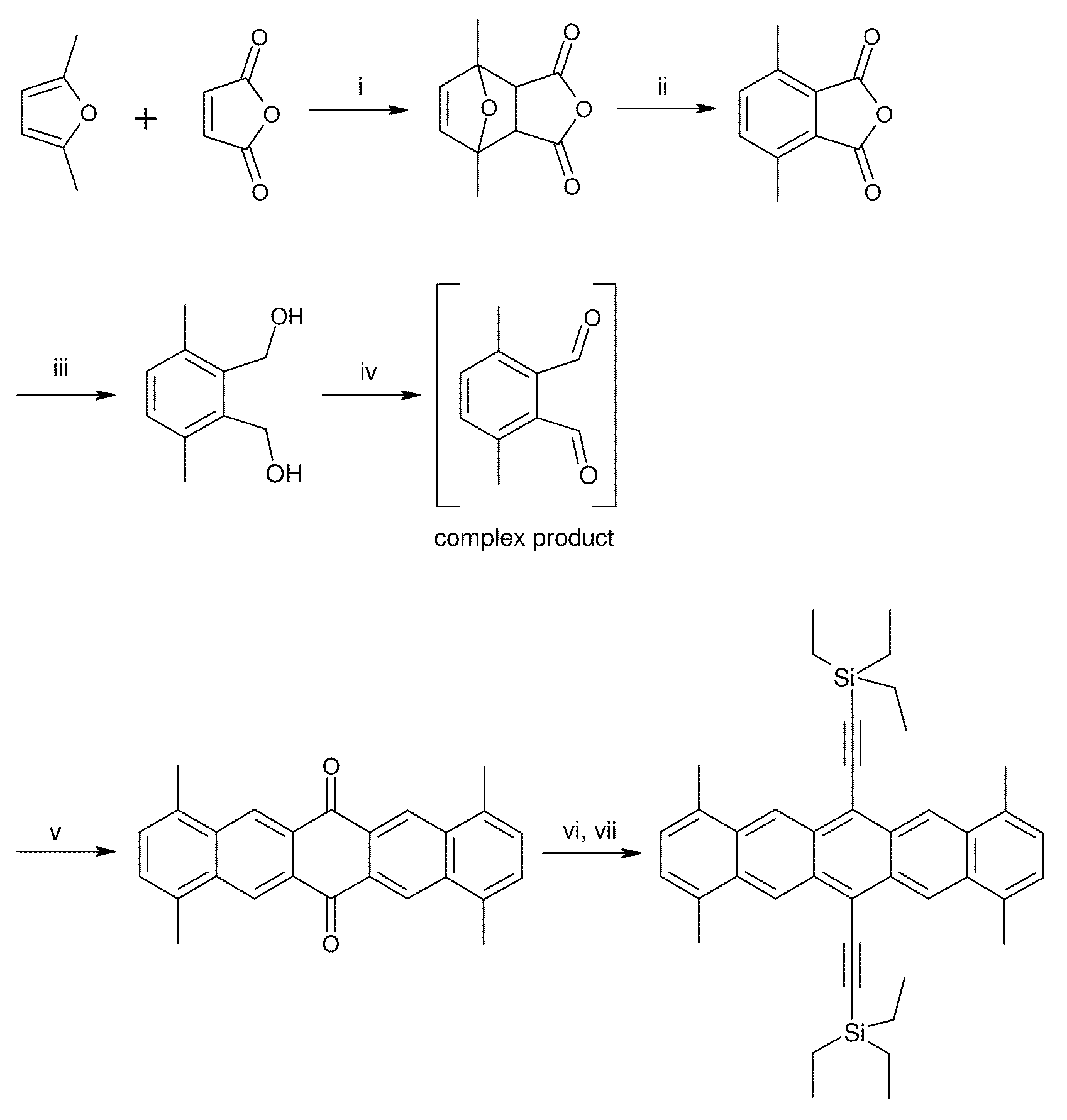
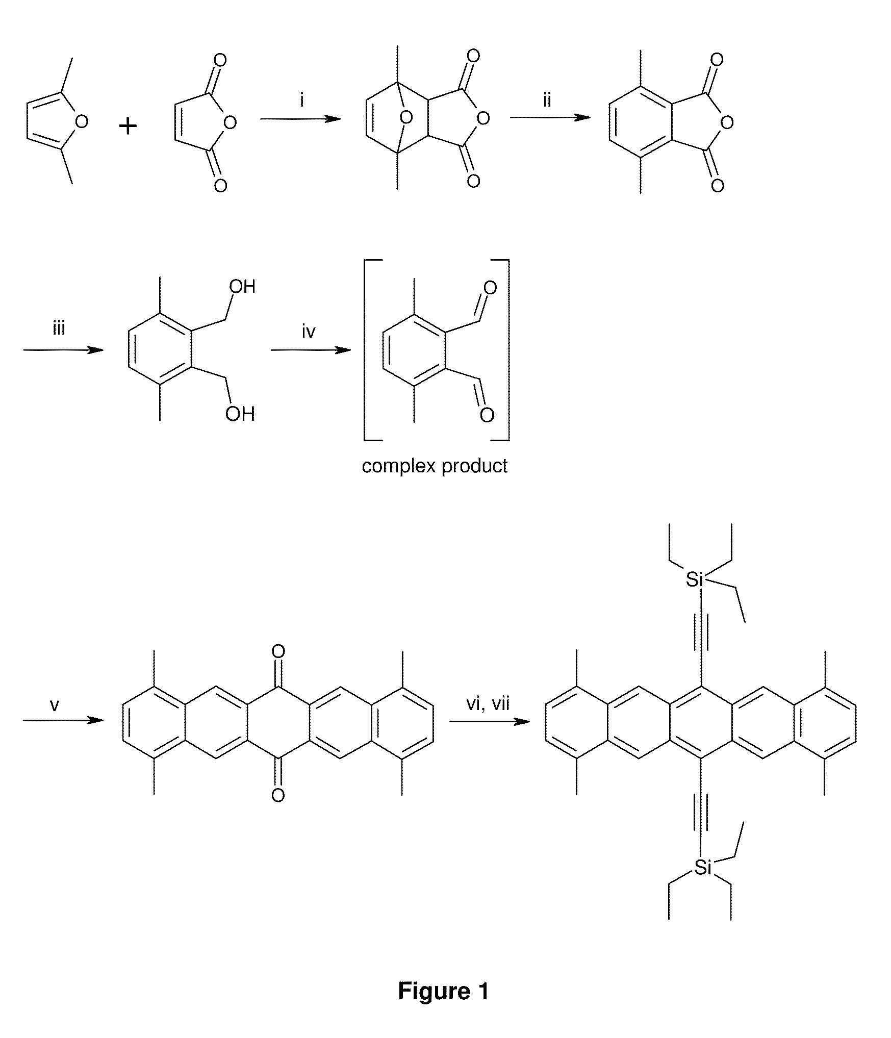
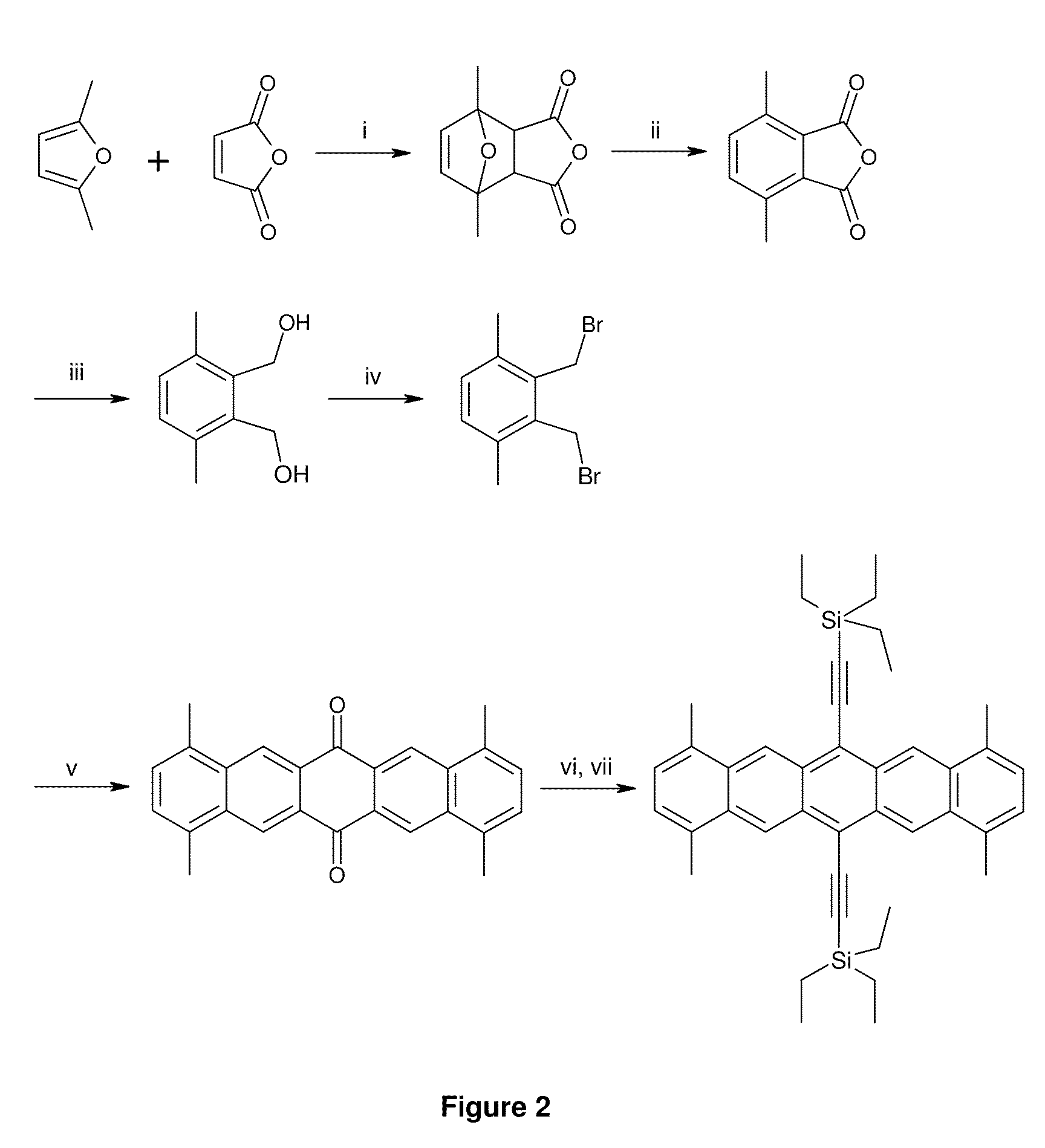
[0177]1,4,8,11-Tetramethyl-6,13-bis(triethylsilylethynyl)pentacene (9) is prepared as described below.

1,7-Dimethyl-4,10-dioxa-tricyclo[5.2.1.02,6]dec-8-ene-3,5-dione 1

[0178]

[0179]A 100 mL 3-necked RBF is fitted with a mechanical stirrer, a condenser and a subaseal, and placed under nitrogen. Maleic anhydride (25.5 g, 0.260 mol) and anhydrous diethyl ether (35 mL) are charged to the RBF. 2,5-Dimethylfuran (27.7 mL, 0.260 mol) is added via syringe over a period of 20 mins to the suspension at 22° C. The reaction mixture is stirred for 18 h. The product is filtered off, washed with cold diethyl ether (100 mL), and dried under vacuum to yield the product 1 as a cream solid (36.32 g, 72%): 1H-NMR (300 MHz, CDCl3) δ 6.35 (s, 2H), 3.16 (s, 2H), 1.76 (s, 6H).

4,7-Dimethyl-isobenzofuran-1,3-dione 2

[0180]

[0181]1,7-Dimethyl-4,10-dioxa-tricyclo[5.2.1.02,6]dec-8-ene-3,5-dione 1 (30.0 g, 0.150 mol) is added slowly in portions to stirred 98% sulfuric acid (300 mL) in a 1 L flange flask cooled to −5...

example 2

[0196]A top gate OFET device as exemplarily shown in FIG. 6 is prepared as described in WO 2005 / 055248 A2. Compound (9) of example 1 is dissolved with the binder material poly(alpha-methylsyrene) (1:1 ratio) at 4% total solids content in tetralin. The resulting solution is spin-coated upon masked Pt / Pd patterned source / drain electrodes on a PEN substrate. A solution of the dielectric material Lisicon™ D139 (commercially available from Merck KGaA, Darmstadt, Germany) is used as the gate insulator layer. A gold gate contact is provided onto the coated and dried gate insulator layer by evaporation through a shadow mask.

[0197]The device performance is measured as described in WO 03 / 052841 A1. FIG. 7 shows the transfer characteristics, mobility and on / off ratio of the OFET. The device shows high mobility and a high on / off ratio:

μlin=6.3 cm2 / Vs (linear mobility)

Ion / Ioff=7×10³ (current on / off ratio)


PUM

PropertyMeasurementUnit
boiling pointaaaaaaaaaa
temperaturesaaaaaaaaaa
boiling pointsaaaaaaaaaa

Abstract

The invention relates to a process of preparing substituted pentacenes, to novel pentacenes prepared by this process, to the use of the novel pentacenes as semiconductors or charge transport materials in optical, electrooptical or electronic devices including field effect transistors (FETs), electroluminescent, photovoltaic and sensor devices, and to FETs and other semiconducting components or materials comprising the novel pentacenes.

Description

FIELD OF INVENTION[0001]The invention relates to a process for preparing substituted pentacenes, and to novel pentacenes prepared by this process. The invention further relates to the use of the novel pentacenes as semiconductors or charge transport materials in optical, electrooptical or electronic devices including field effect transistors (FETs), electroluminescent, photovoltaic and sensor devices. The invention further relates to FETs and other semiconducting components or materials comprising the novel pentacenes.BACKGROUND AND PRIOR ART[0002]In recent years, there has been development of organic semiconducting materials in order to produce more versatile, lower cost electronic devices. Such materials find application in a wide range of devices or apparatus, including organic field effect transistors (OFETs), organic light emitting diodes (OLEDs), photodetectors, photovoltaic (PV) cells, sensors, memory elements and logic circuits to name just a few. The organic semiconducting ...

Claims


Application Information

Patent Timeline
Patent Type & Authority Applications(United States)
IPC IPC(8): H01B1/12C07F7/08C09K11/06
CPCC07F7/0809H01L51/0094C07F7/0805H10K85/40C07F7/08C09K11/59H01L21/18H10K10/00
Inventor TIERNEY, STEVENHEENEY, MARTINBAILEY, CLAREZHANG, WEIMIN
Owner FLEHKSENEHBL LTD
Why Eureka
Try Eureka