Increasing LCD aperture ratios

a technology of aperture ratio and display panel, applied in the field of display panel, can solve the problems of large viewing angle of lcds and relatively narrow viewing angle, and achieve the effect of improving the aperture ratio of the display and reducing the display aperture ratio

Inactive Publication Date: 2010-05-27
PARK TAE HYEONG +2
View PDF8 Cites 9 Cited by
  • Summary
  • Abstract
  • Description
  • Claims
  • Application Information

AI Technical Summary

Benefits of technology

[0007]In accordance with the exemplary embodiments disclosed herein, LCDs with higher brightness are provided in which the improvement in brightness is achieved by minimizing the amount of reduction in the aperture ratio of the LCDs that otherwise result from the above measures taken to increase their viewing angles.
[0014]In accordance with the exemplary embodiments described herein, the reduction in display aperture ratio that results from the implementation of viewing-angle-improving features in the display is minimized, thereby improving the aperture ratio of the display. A better understanding of the above and many other features and advantages of the novel higher-brightness LCDs of the present invention may be obtained from a consideration of the detailed description of some exemplary embodiments thereof below, particularly if such consideration is made in conjunction with the appended drawings, wherein like reference numerals are used to identify like elements illustrated in one or more of the figures thereof

Problems solved by technology

VA mode LCDs share a major drawback with other types of LCDs, namely, a relatively narrow viewing angle.

Method used


Image

  • Increasing LCD aperture ratios
  • Increasing LCD aperture ratios
  • Increasing LCD aperture ratios

Examples


Embodiment Construction

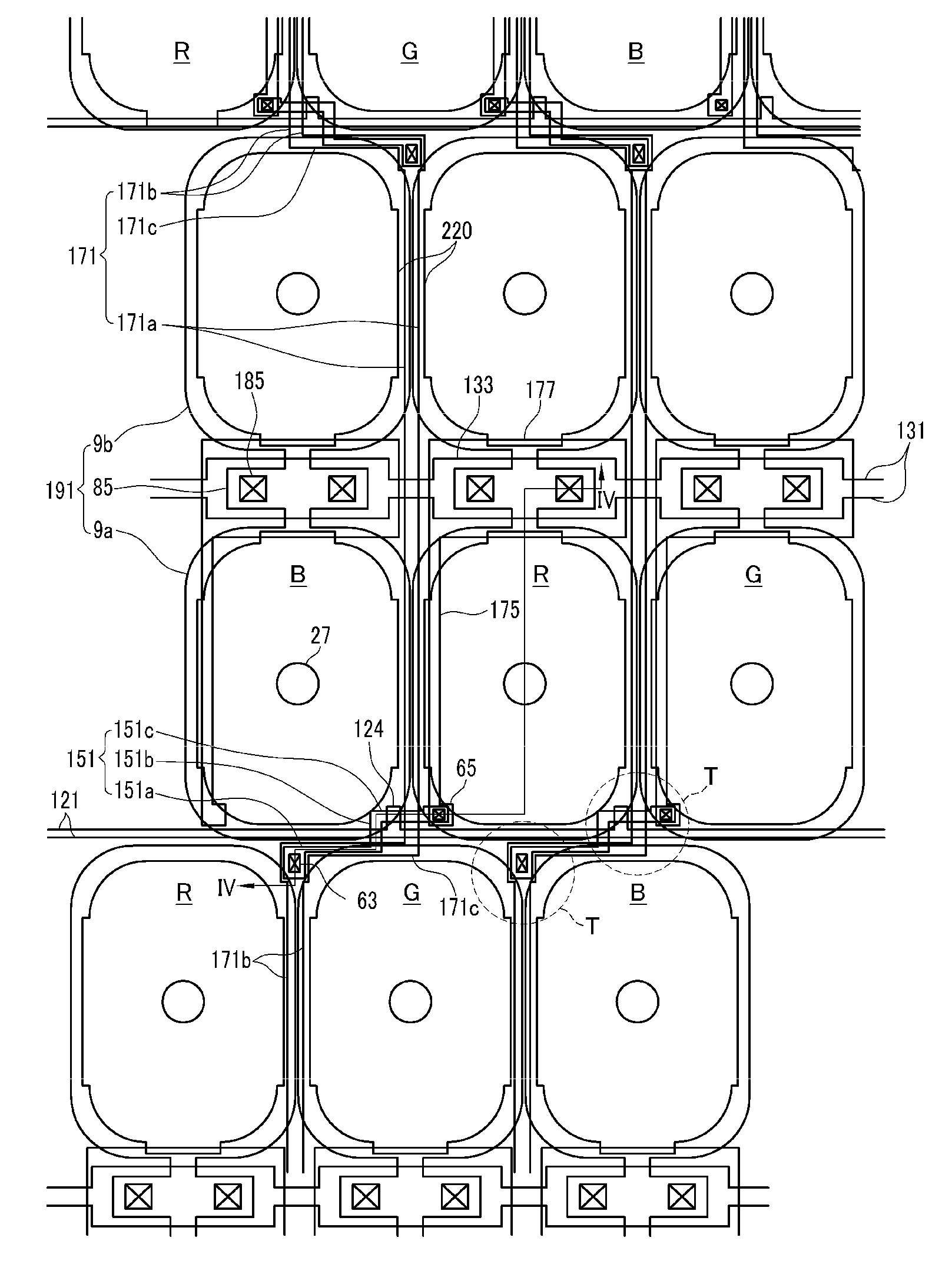
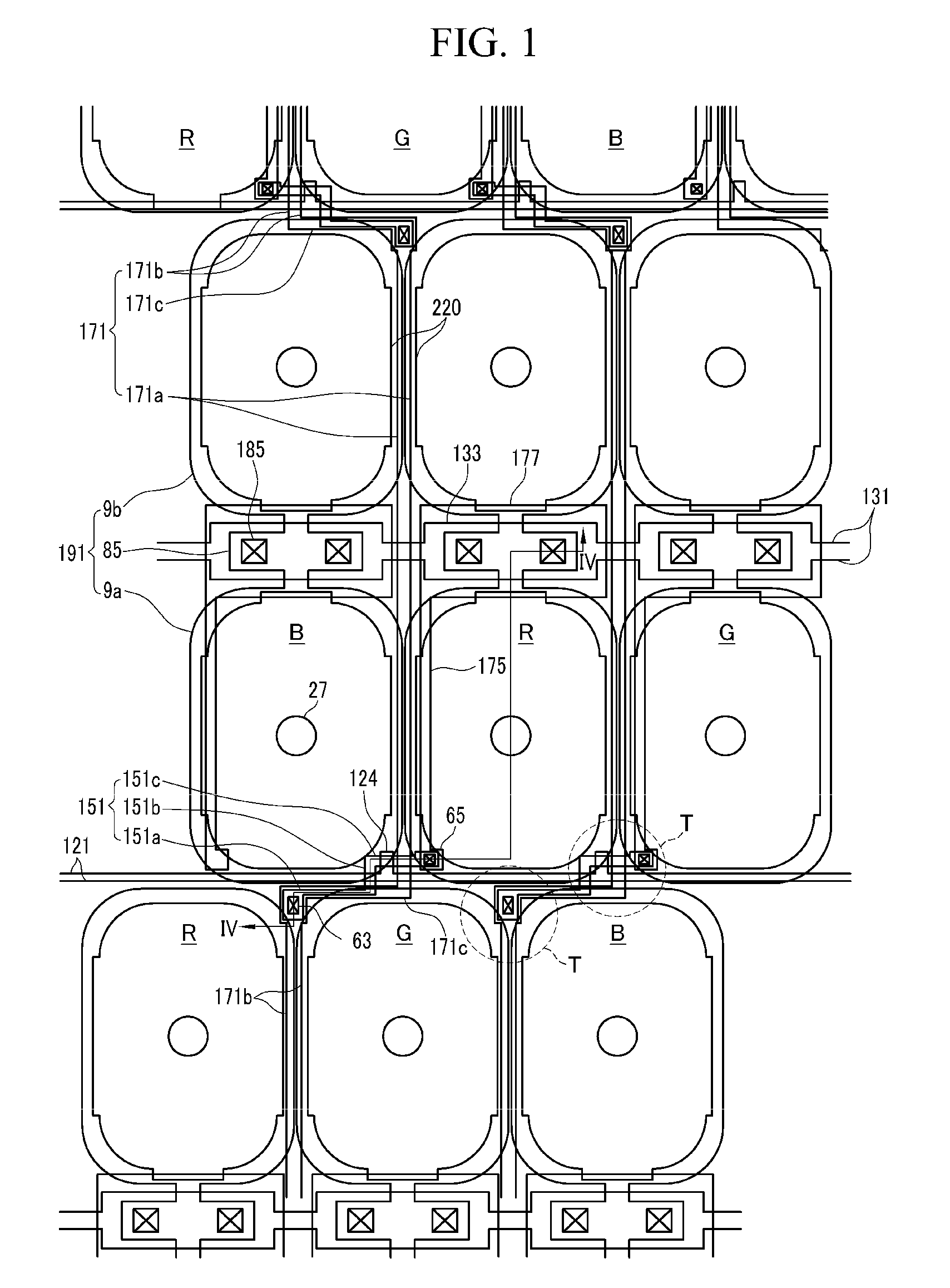
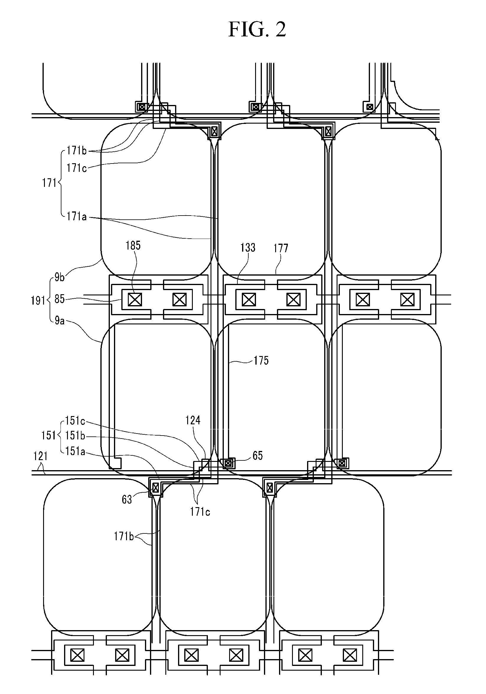
[0021]The present invention is described more fully hereinafter with reference to the accompanying drawings, in which exemplary embodiments thereof are shown. As those skilled in the art will appreciate, the described embodiments can be modified in various ways, all without departing from the spirit or scope of the present invention.

[0022]In the drawings, the thickness of layers, films, panels, regions, and the like may be exaggerated for clarity. Like reference numerals are used to designate like elements throughout the specification. Also, it should be understood that when an element, such as a layer, film, region, or substrate, or the like, is described as being “on” another element, it is meant that the first element may be disposed directly on the other element, or alternatively, that intervening elements may also be present. Conversely, when an element is described as being disposed “directly on” another element, it is meant that no intervening elements are present.

[0023]An ex...


PUM

PropertyMeasurementUnit
angleaaaaaaaaaa
dielectric constantaaaaaaaaaa
inclination angleaaaaaaaaaa

Abstract

A liquid crystal display includes an insulating substrate, a semiconductor, a gate insulating layer, a gate line, an interlayer insulating layer, a data line, a drain electrode, a passivation layer, and a pixel electrode. The semiconductor is formed on the insulating substrate and includes source, drain, and channel regions. The gate line is formed on the gate insulating layer over the semiconductor, and overlaps the channel region thereof. The data line is formed on the interlayer insulating layer and has a source electrode electrically connected to the source region and a drain electrode electrically connected to the drain region. The passivation layer is formed on the data line and drain electrode. The pixel electrode is formed on the passivation layer, and electrically connected to the drain electrode. The data line overlaps the drain region.

Description

RELATED APPLICATIONS[0001]This application is a divisional of U.S. patent application Ser. No. 11 / 980,857, filed on Oct. 30, 2007, which claims priority of Korean Patent Application No. 10-2006-0116853, filed Nov. 24, 2006, the entire disclosure of which is incorporated herein by reference.BACKGROUND[0002]This disclosure relates to display panels in general, and more particularly, to display panels for liquid crystal displays (LCDs) having improved aperture ratios.[0003]LCDs constitute one of the more widely used types of flat panel displays (FPDs), and typically include two display panels on which field generating electrodes, such as pixel electrodes and a common electrode, are respectively formed, with a layer of a liquid crystal material interposed between the two panels. A voltage is applied to the field generating electrodes to generate an electric field in the liquid crystal layer, which determines the orientation of the molecules of the liquid crystal layer therebetween and t...

Claims


Application Information

Patent Timeline
Patent Type & Authority Applications(United States)
IPC IPC(8): G02F1/136
CPCG02F1/133707G02F1/134336G02F2201/40G02F1/136286G02F2001/134345G02F1/1362G09G2300/0426G02F1/134345G02F1/1343G02F1/136
Inventor PARK, TAE-HYEONGPARK, JOON-HALEE, SO-HYUN
Owner PARK TAE HYEONG
Why Eureka
Try Eureka