Power semiconductor module

a technology of power semiconductor modules and semiconductor modules, which is applied in the manufacture of printed circuits, solid-state devices, basic electric elements, etc., can solve the problems of large-sized power, and hinder the size reduction of power semiconductor modules

Inactive Publication Date: 2010-06-03
MITSUBISHI ELECTRIC CORP
View PDF29 Cites 24 Cited by
  • Summary
  • Abstract
  • Description
  • Claims
  • Application Information

AI Technical Summary

Benefits of technology

[0020]A power semiconductor module according to the present invention includes: a lead frame; a power semiconductor element; and a cylindrical conductor. A part of the lead frame, the power semiconductor element, and the cylindrical conductor are all sealed with transfer molding resin. Terminal portions of the lead frame protrude from peripheral side portions of the p

Problems solved by technology

This hinders size reduction of the power semiconductor module.
This problem is particularly prominent in power semiconductor modules having a large number of terminals, or in power semiconductor modules having a large current carrying capacity and terminals with a large width.
This also results in

Method used


Image

  • Power semiconductor module
  • Power semiconductor module
  • Power semiconductor module

Examples


first embodiment

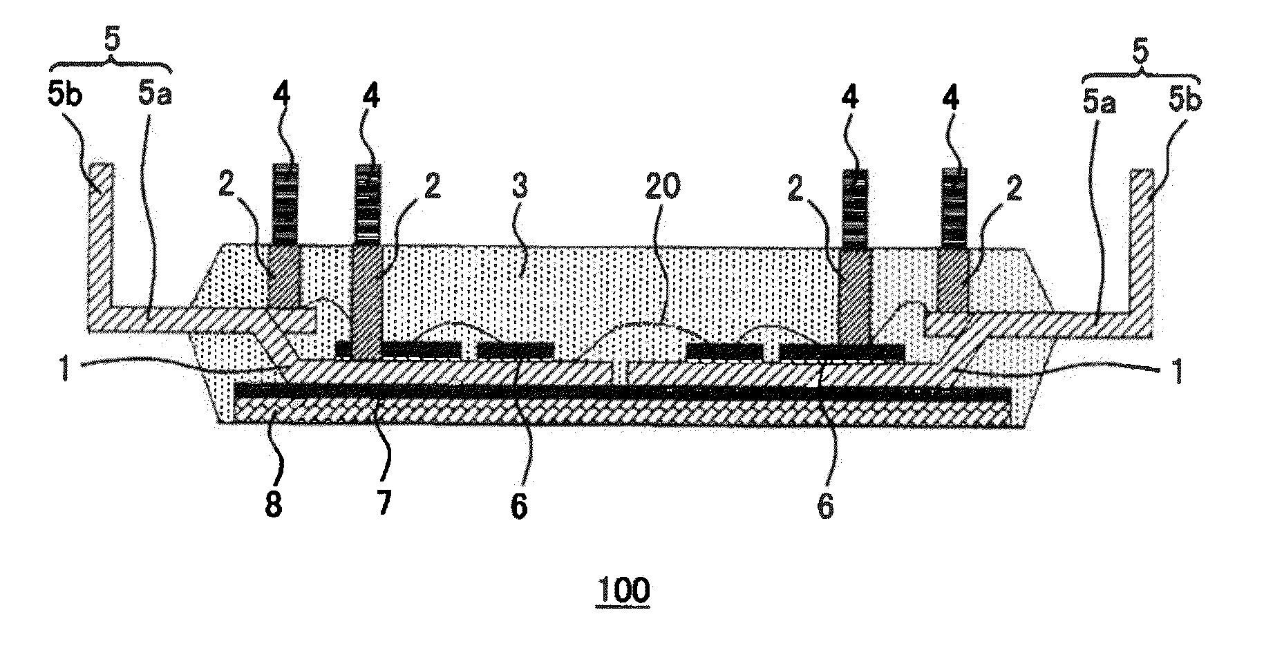
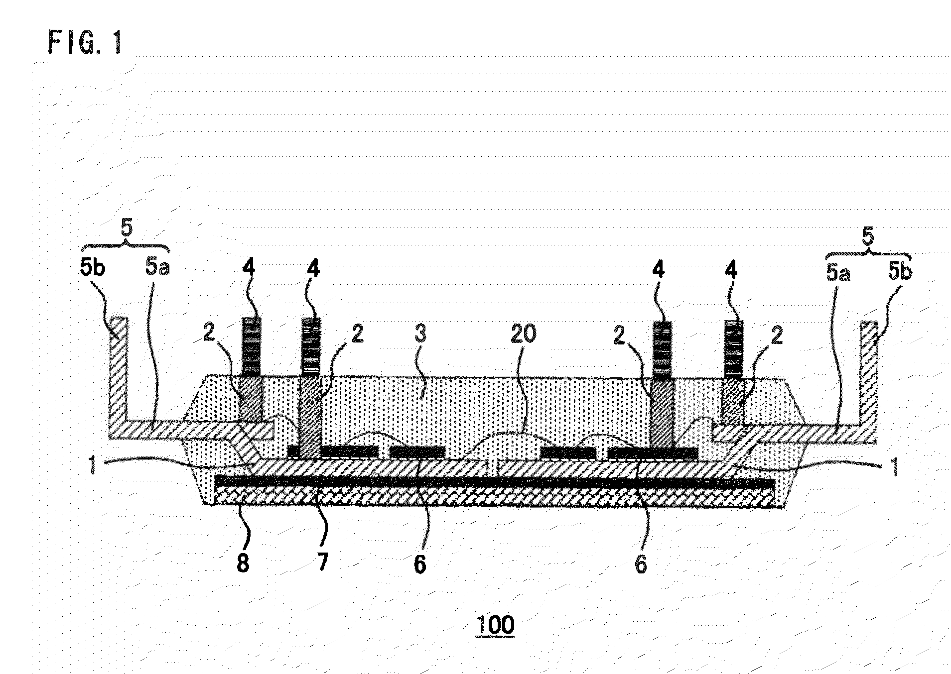
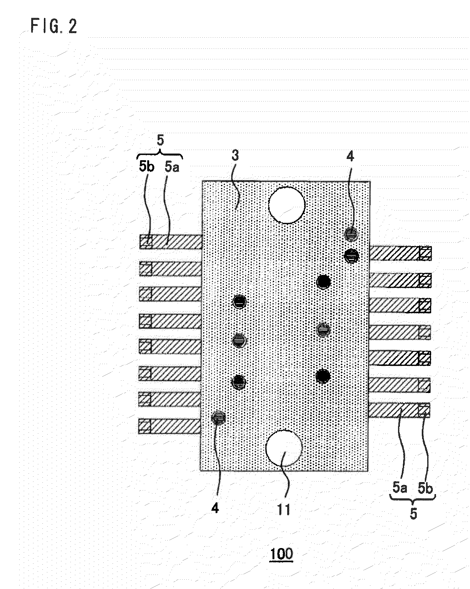
[0032]FIG. 1 is a schematic cross-sectional view showing a power semiconductor module according to the first embodiment of the present invention.

[0033]As shown in FIG. 1, in a power semiconductor module 100 of the present embodiment, power semiconductor elements 6 are mounted on one surface of a lead frame 1. The other surface of the lead frame 1, which is opposite to said one surface having the power semiconductor elements 6 mounted thereon, is joined to a metal base plate 8 via an insulation sheet 7 having high thermal conductivity, which insulation sheet 7 is interposed between the said other surface and the metal base plate 8. Metal cylinders 2, which are cylindrical conductors each having a hole and each acting as a terminal, are joined to the lead frame 1 so as to be substantially perpendicular to said one surface of the lead frame 1. The power semiconductor elements 6 and the metal cylinders 2 are joined to a wiring pattern on the lead frame 1 respectively. In this state, the...

second embodiment

[0068]FIG. 6 is a schematic cross-sectional view of a power semiconductor module according to the second embodiment of the present invention.

[0069]As shown in FIG. 6, in a power semiconductor module 200 of the present embodiment, a ceramic circuit substrate 9 is used, which includes: a ceramic plate 9b, a copper foil 9a that is a metal body provided on one surface of the ceramic plate 9b, and a copper wiring pattern 9c provided on the other surface of the ceramic plate 9b. The power semiconductor module 200 of the present embodiment is the same as the power semiconductor module 100 of the first embodiment except that the power semiconductor elements 6 and the metal cylinders 2 are mounted on the wiring pattern 9c of the ceramic circuit substrate 9, and that the said other surface of the lead frame 1 is joined to the wiring pattern 9c.

[0070]In the power semiconductor module 200 of the present embodiment, the respective components are joined to the wiring pattern 9c of the ceramic ci...

third embodiment

[0071]FIG. 7 is a schematic cross-sectional view showing a power semiconductor module according to the third embodiment of the present invention.

[0072]As shown in FIG. 7, in a power semiconductor module 300 of the present embodiment, a metal circuit substrate 10 is used, which includes a metal plate 10a and a metallic foil wiring pattern 10c that is provided above one surface of the metal plate 10a while a resin insulation layer 10b is interposed between the wiring pattern 10c and the metal plate 10a. The power semiconductor module 300 is the same as the power semiconductor module 100 of the first embodiment except that the power semiconductor elements 6 and the metal cylinders 2 are mounted on the wiring pattern 10c of the metal circuit substrate 10, and that the said other surface of the lead frame 1 is jointed to the wiring pattern 10c.

[0073]In the power semiconductor module 300 of the present embodiment, since the respective components are joined to the wiring pattern 10c of th...


PUM


Abstract

A wiring process between the provided power semiconductor module and the external circuit is simple. In the power semiconductor module, a power semiconductor element and a cylindrical conductor are joined to one surface of a lead frame. An opening of the cylindrical conductor is exposed at a surface of transfer molding resin. Sealing with the transfer molding resin is performed such that terminal portions of the lead frame protrude from peripheral side portions of the transfer molding resin. The cylindrical conductor is conductive with a control circuit. The terminal portions of the lead frame are each conductive with a main circuit.

Description

BACKGROUND OF THE INVENTION[0001]1. Field of the Invention[0002]The present invention relates to a resin-sealed power semiconductor module, formed by transfer molding, which is excellent in terms of productivity. The present invention particularly relates to a resin-sealed power semiconductor module, formed by transfer molding, which is small in size and which realizes large-current operation.[0003]2. Description of the Background Art[0004]A power semiconductor module that is: small in size;[0005]capable of efficiently discharging heat generated by its operation, to the outside; and capable of operating with a large current, is a power semiconductor module sealed with resin by transfer molding.[0006]One of such power semiconductor modules sealed with resin by transfer molding is the one in which: a power semiconductor element is mounted on one surface of a lead frame; a metal substrate that includes an aluminum plate or copper plate and includes a high thermal conductive insulation ...

Claims


Application Information

Patent Timeline
IPC IPC(8): H01L23/495
CPCH01L23/3107H01L2224/73265H01L23/4334H01L23/49517H01L23/49531H01L23/49575H01L25/16H01L2224/48091H01L2224/48137H01L2224/48247H01L2924/01078H01L2924/19041H05K1/141H05K1/145H05K3/202H01L23/3735H01L2224/45124H01L2924/01068H01L24/48H01L2924/00014H01L2924/00H01L24/45H01L2924/181H01L2224/49109H01L24/49H01L2924/00012
Inventor OKA, SEIJIOBIRAKI, YOSHIKOOI, TAKESHI
Owner MITSUBISHI ELECTRIC CORP
Why Eureka
Try Eureka