

Semiconductor integrated circuit device
a technology of integrated circuit and semiconductor, applied in the direction of semiconductor/solid-state device testing/measurement, semiconductor device details, semiconductor/solid-state device testing/measurement, etc., can solve problems such as kirkendall void and connection failur
- Summary
- Abstract
- Description
- Claims
- Application Information
AI Technical Summary
Benefits of technology
Problems solved by technology
Method used
Image

Examples
Embodiment Construction
Summary of Preferred Embodiments
[0063]First, representative preferred embodiments of the invention disclosed in the present application will be summarized below.
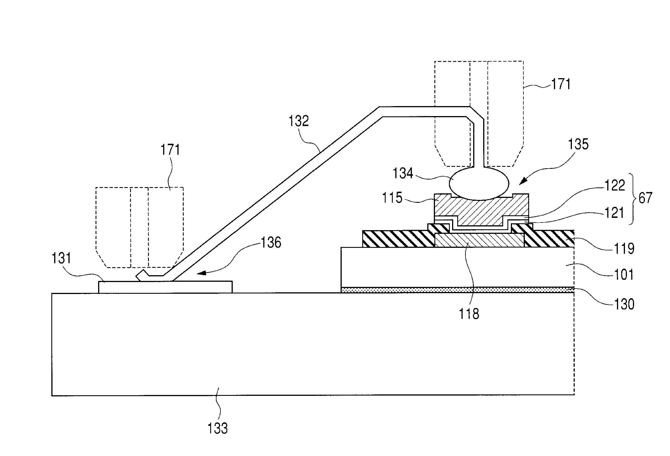
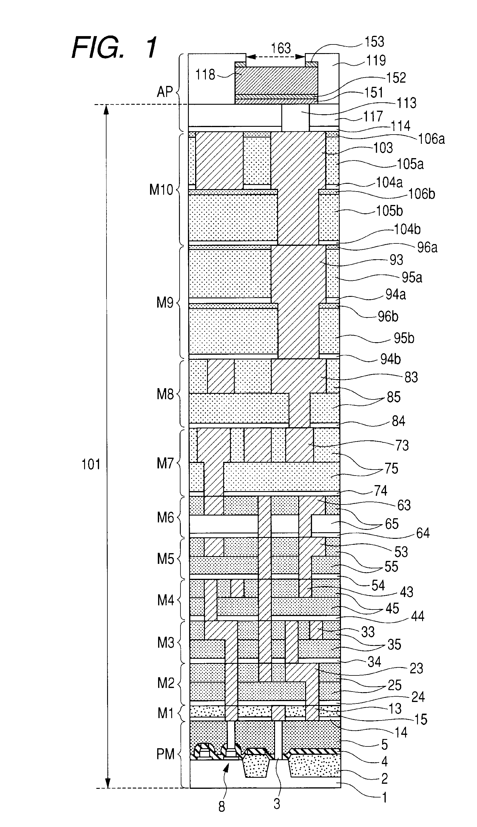
[0064]1. A semiconductor integrated circuit device includes: (a) an aluminum or copper-based pad electrode provided over a device surface of a semiconductor chip; (b) a barrier metal film provided over the pad electrode; (c) a surface metal film provided over the barrier metal film, and including gold as a principal component; and (d) a bonding ball or bonding wire bonded to the surface metal film, and including gold or copper as a principal component.
[0065]2. In the semiconductor integrated circuit device according to Item 1, a thickness of the surface metal film is larger than that of the barrier metal film.
[0066]3. In the semiconductor integrated circuit device according to Item 1 or 2, the surface metal film is formed by electrolytic plating or sputtering.
[0067]4. In the semiconductor integrated circuit device according ...
PUM
 Abstract
Description
Claims
Application Information