

Self-Assembled Electrical Contacts
a technology of electrical contacts and self-assembling, which is applied in the direction of sustainable manufacturing/processing, final product manufacturing, printed circuit manufacturing, etc., can solve the problems of individual devices, inability to handle and deterministically place components with reasonable efficiency and cost, and inability to meet the needs of small components
- Summary
- Abstract
- Description
- Claims
- Application Information
AI Technical Summary
Benefits of technology
Problems solved by technology
Method used
Image

Examples
Embodiment Construction
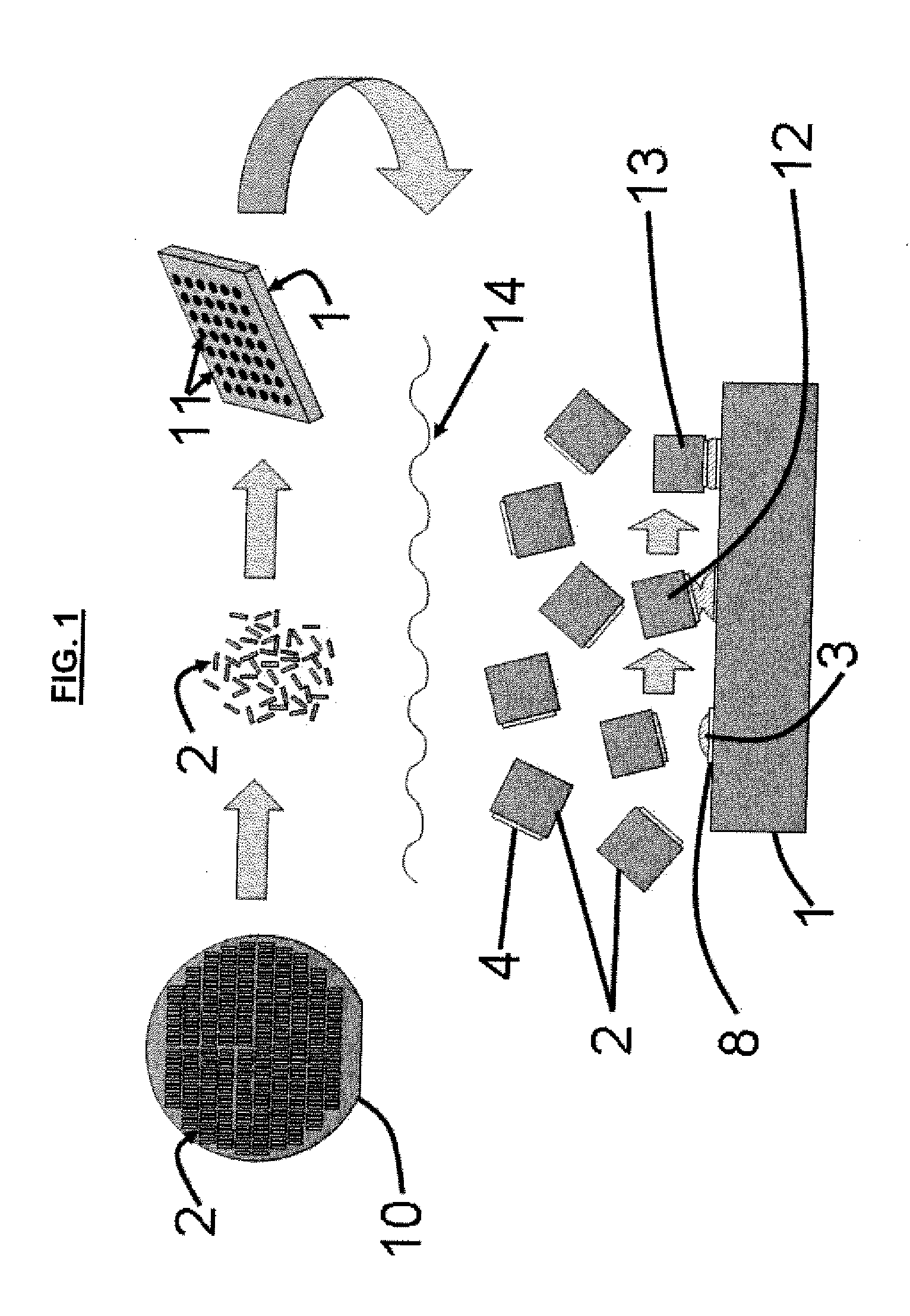
[0031]The embodiments herein and the various features and advantageous details thereof are explained more fully with reference to the non-limiting embodiments that are illustrated in the accompanying drawings and detailed in the following description. Descriptions of well-known components and processing techniques are omitted so as to not unnecessarily obscure the embodiments herein. The examples used herein are intended merely to facilitate an understanding of ways in which the embodiments herein may be practiced and to further enable those of skill in the art to practice the embodiments herein. Accordingly, the examples should not be construed as limiting the scope of the embodiments herein.
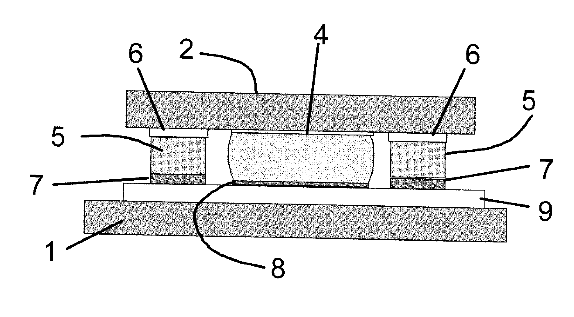
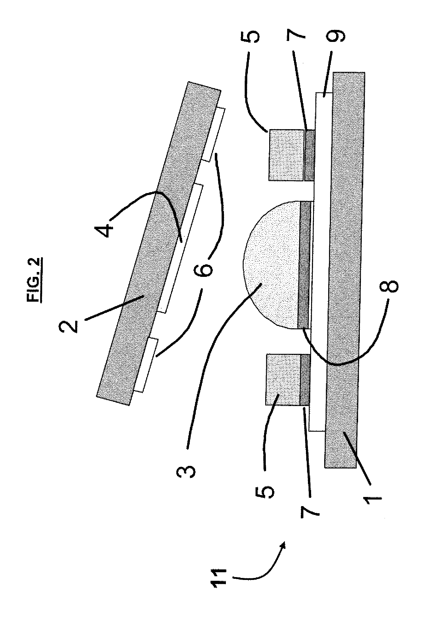
[0032]The embodiments herein provide a technique for forming electrical and mechanical connections via self-assembly without sacrificing the electrical qualities of those connections on microscale-sized parts (e.g., approximately 280 μm). The use of two alloys, or more generally the use of two ...
PUM
| Property | Measurement | Unit |
|---|---|---|
| size | aaaaa | aaaaa |
| size | aaaaa | aaaaa |
| diameter | aaaaa | aaaaa |
Abstract
Description
Claims
Application Information