


Quick Research
Generate reliable direction feasibility study reports for your R&D in just a few steps.

Technical Q&A
Discover and master advanced knowledge NOW. Basics, ideas, possibilities, all at once.

Find Solutions
As an expert in R&D theories, this can generate solutions to your technical problems instantly.

Evaluate Feasibility
Analyze your overall solution with one click, know your potential R&D risks in advance.

Monitor Landscape
Get weekly tech updates, stay abreast of the latest tech innovations and key insights.
Semiconductor device
a technology of semiconductor devices and capacitors, applied in the field of semiconductor devices, can solve the problems of suppressing the noise of capacitors, and achieve the effect of reducing noise and excellent layout efficiency
- Summary
- Abstract
- Description
- Claims
- Application Information
AI Technical Summary
Benefits of technology
Problems solved by technology
Method used
Image

Examples
first embodiment
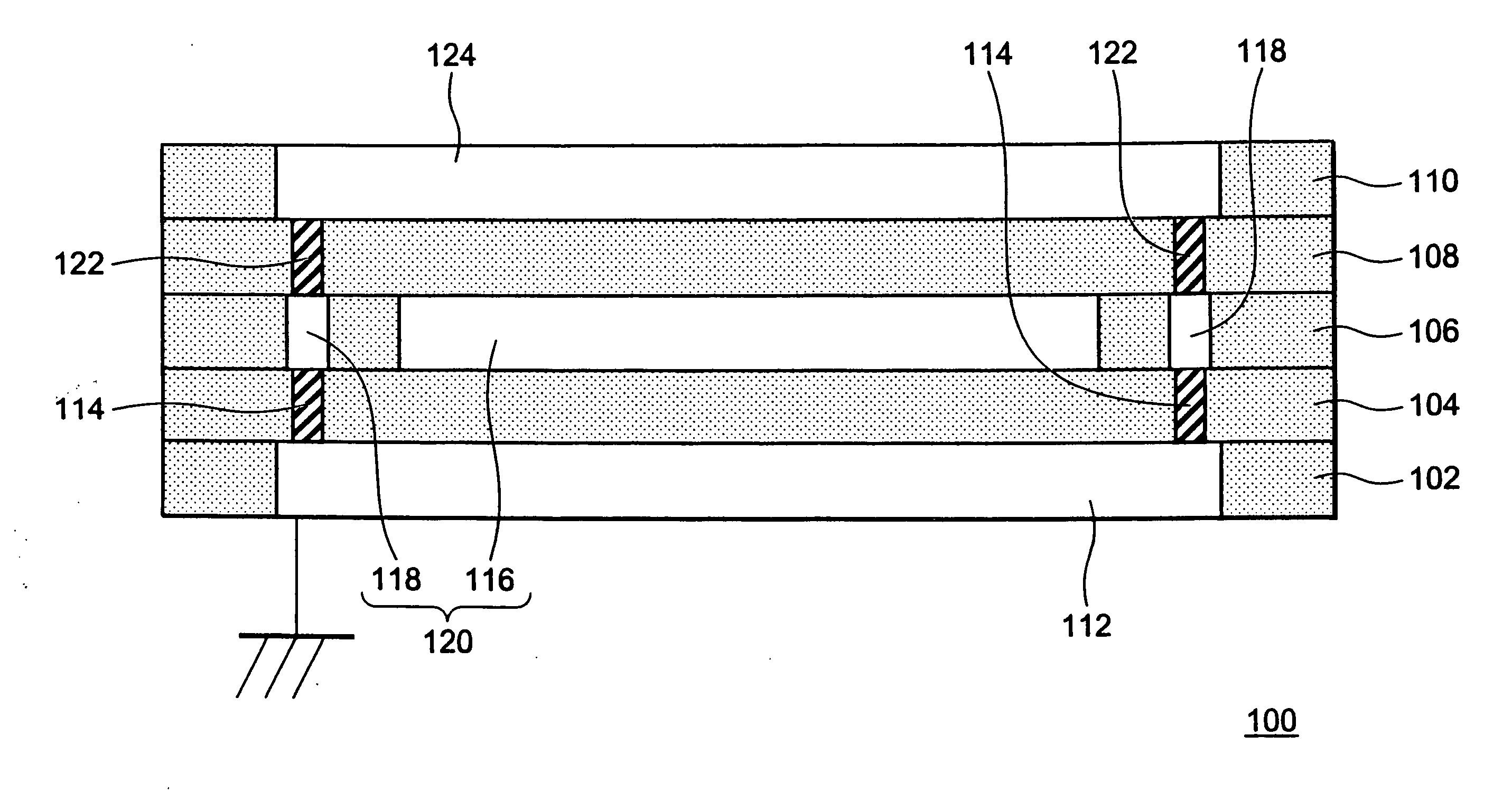
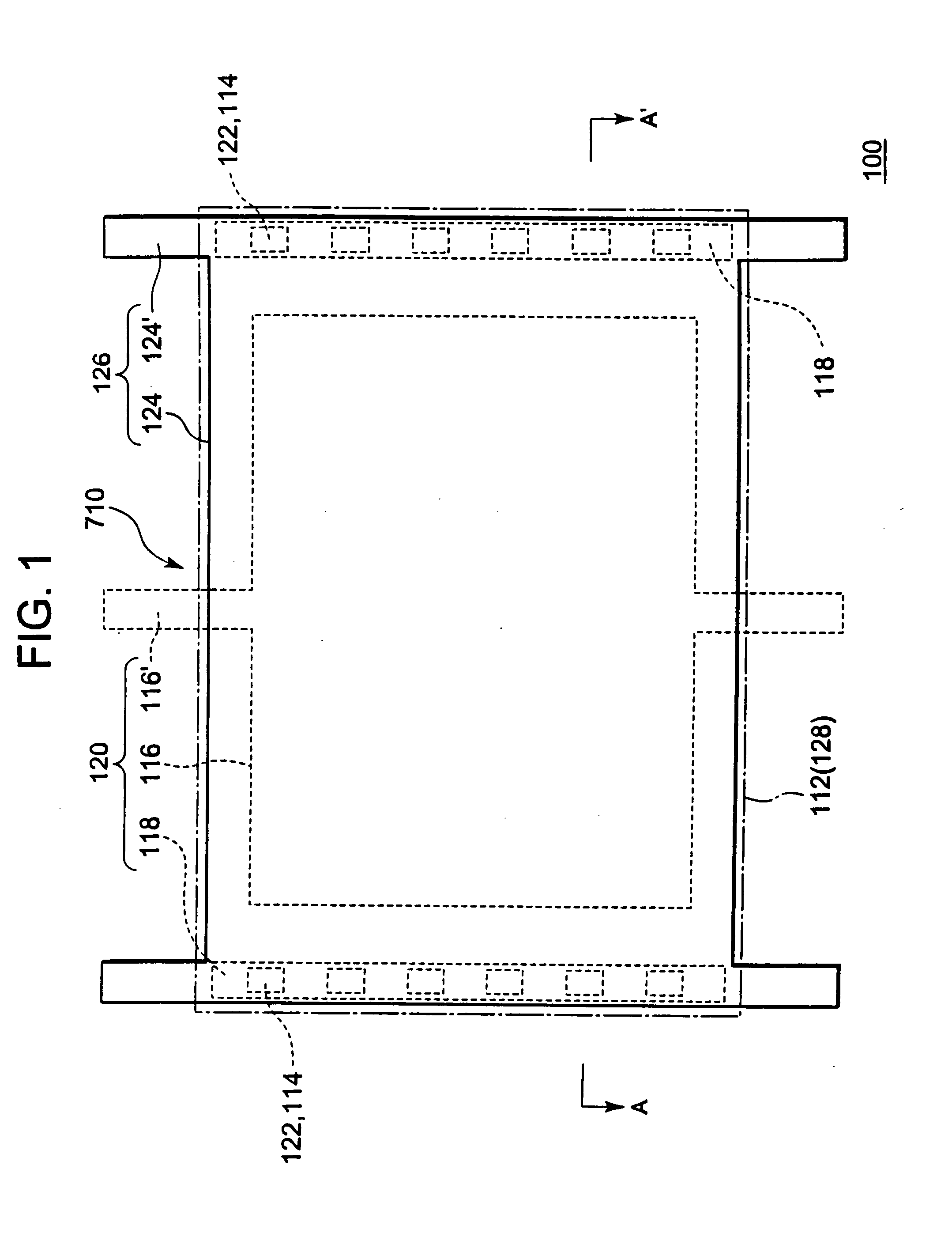
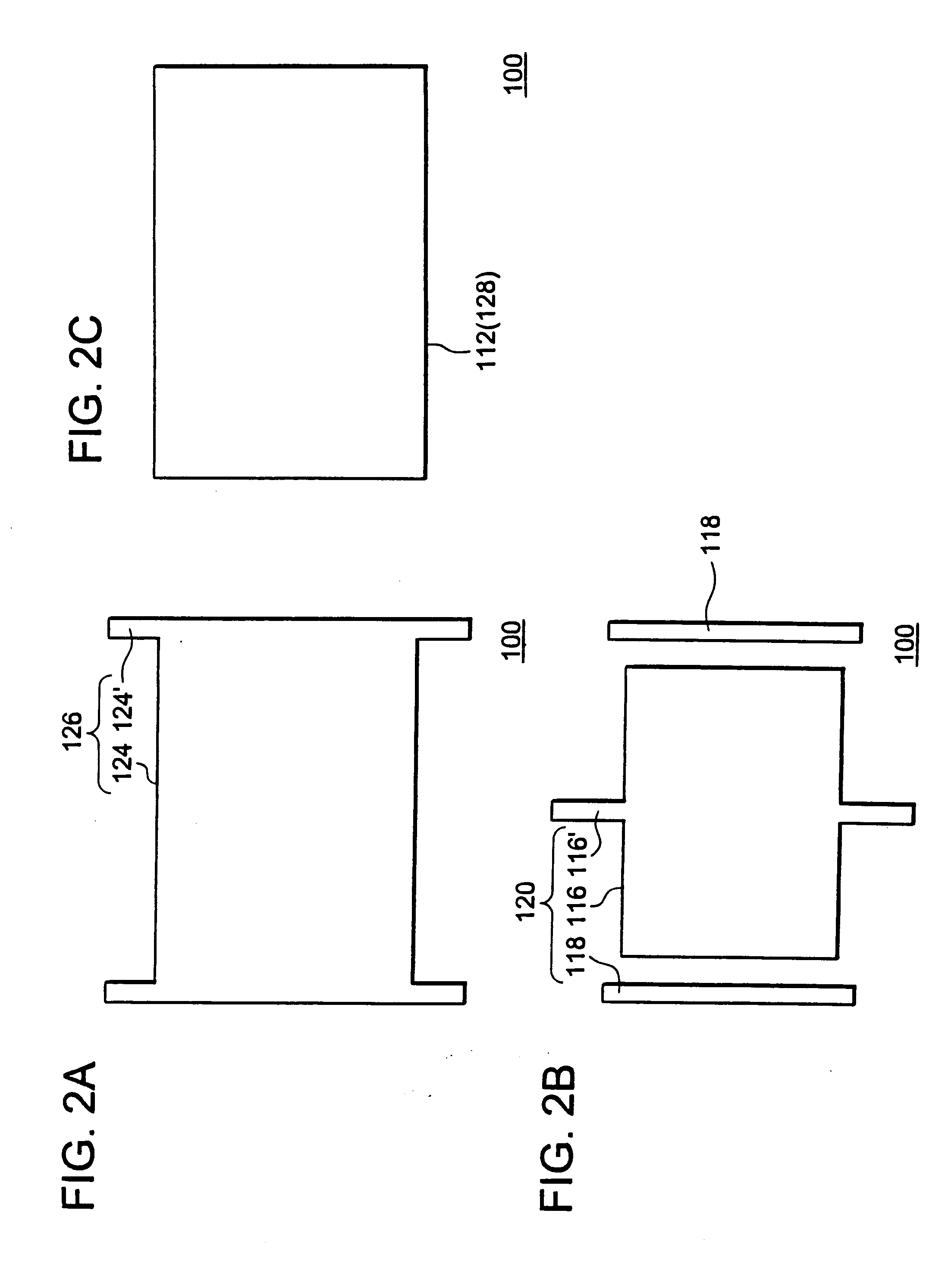
[0034]FIGS. 1 to 3 and 16 are views for describing a first embodiment of the present invention. Referring to FIG. 16, a transistor composed of a gate 910, a diffusion layer 920 and an element separation 930, and other parts are constructed on a substrate 900 of a semiconductor device 100; and a contact 940, a line 945 and the like are formed in insulating films 950 and 960. A first wiring layer 128 including a lower electrode 112 is buried in a first interlayer insulating film 102 on an insulating film 961.
[0035]The semiconductor device 100 according to the first embodiment of the present invention comprises: a first capacitor 710 including an upper electrode 124, a lower electrode 112, an intermediate electrode 116 arranged between the upper electrode 124 and the lower electrode 112, and a first shield line 118 arranged in the same layer as the intermediate electrode 116; and a second capacitor 720, including an upper electrode 124, a lower electrode 112, and an intermediate electr...
second embodiment
[0062]FIGS. 5 to 7 are views showing a second embodiment of the present invention. FIG. 5 is a plan view illustrating a semiconductor device 200 including a first capacitor 712 according to the second embodiment of the present invention; FIGS. 6A to 6C are plan views illustrating each of the wiring layers; and FIG. 7 is a cross-sectional view along the line A-A′ of FIG. 5.
[0063]The difference of the second embodiment from the first embodiment lies in that the upper electrode 124, the intermediate electrode 116 and the lower electrode 112 constituting the first capacitor 712 have slit-shaped hollows 202, 204 and 206. An explanation of other aspects not different from the first embodiment is omitted.
[0064]The upper electrode 124 included in the third wiring layer 126 has, as illustrated in FIGS. 5 and 6A, the slit-shaped hollow 202; and this part of the slit-shaped hollow 202 is, as illustrated in FIG. 7, composed of the fifth interlayer insulating film 110.
[0065]The intermediate elec...
third embodiment
[0069]FIGS. 9 to 12 are views showing a third embodiment of the present invention. FIG. 9 is a plan view illustrating a semiconductor device 300 including a first capacitor 713 according to the third embodiment of the present invention; FIGS. 10A to 10C are plan views illustrating each of the wiring layers; FIG. 11 is a cross-sectional view along the line A-A′ of FIG. 9; and FIG. 12 is a cross-sectional view along the line B-B′ of FIG. 9.
[0070]The difference of the third embodiment from the first embodiment lies in that the upper electrode 124 and the lower electrode 112 constituting a first capacitor 713 are also electrically connected via a third via 304, a first shield line 302 and a fourth via 306. An explanation of other aspects not different from the first embodiment is omitted.
[0071]The semiconductor device 300 further includes, as illustrated in FIGS. 9 to 12, a first shield line 302 included in the second wiring layer 120, the third via 304 buried in the second interlayer i...
PUM
 Abstract
Description
Claims
Application Information
 - R&D Engineer
- R&D Manager
- IP Professional
- Industry Leading Data Capabilities
- Powerful AI technology
- Patent DNA Extraction
Browse by: Latest US Patents, China's latest patents, Technical Efficacy Thesaurus, Application Domain, Technology Topic, Popular Technical Reports.
© 2024 PatSnap. All rights reserved.Legal|Privacy policy|Modern Slavery Act Transparency Statement|Sitemap|About US| Contact US: help@patsnap.com